- HOME
- Products & Services
- Inspection
- Wafer Pattern Defect Inspection Systems
Products & Services
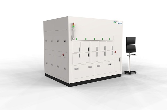
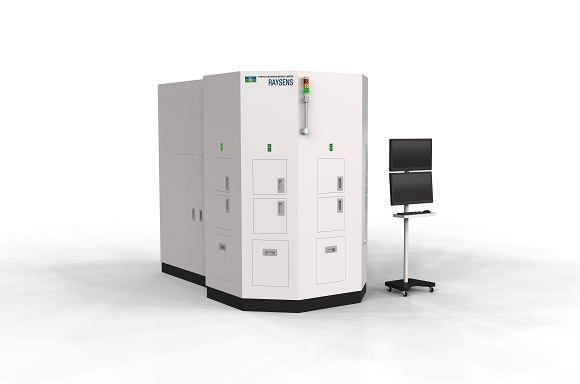
Wafer Pattern Defect Inspection Systems
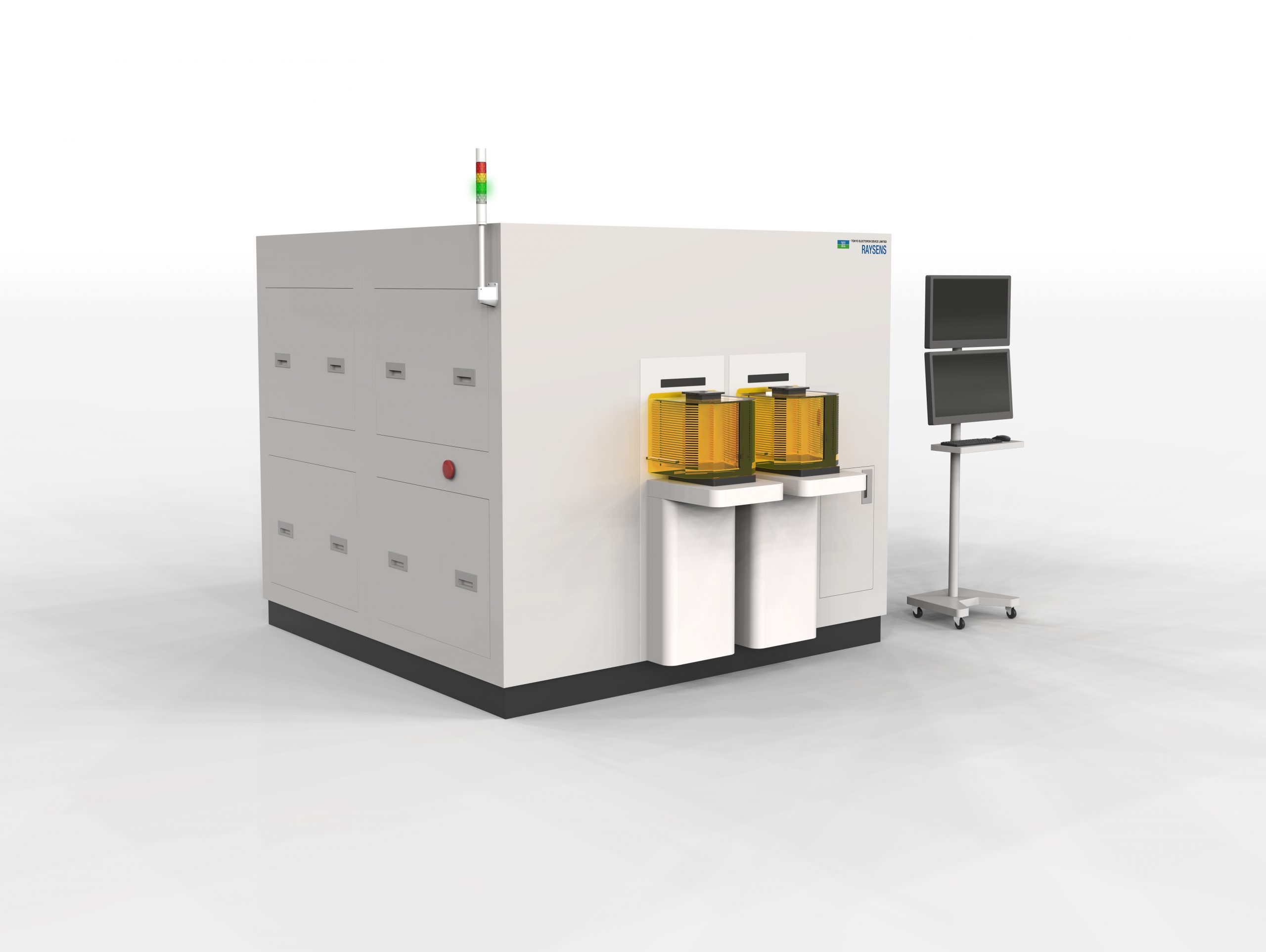
The semiconductor shortage is partly due to supply constraints in legacy nodes, which produce diverse products in small quantities using depreciated equipment. With increasing demand from next-generation devices like IoT, automotive EVs, and XR, bolstering production capacity is crucial. We offer advanced legacy node device inspection equipment, integrating the latest hardware and software inspection technologies, to help address these challenges. Click here for the Japanease site
- Application
- Target Defects
- Features
- Specification
- Sample Evaluation
- Glossary
- 【Spotlight】Revolutionizing AI Chips
Application
・Main Target Devices: MEMS, Power, Analog
・Various Device Wafer: Inspection of appearance defects such as film deposition, resist development, and pattern defects after etching.
(Target Wafer Materials: Si, SiC, GaN, InP, LT/LN, Glass, Resin)
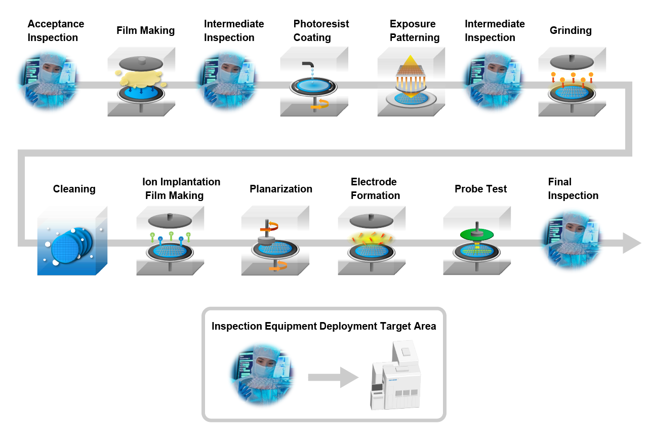
Candidate Introduction Inspection Process
Target Defects
・Surface:Scratches, cracks, dimples, chippings, protrusions, particles, dirt, diffraction, blemishes and irregularities
Features
High-Speed, High-Sensitivity Inspection
Utilizing a specially developed ultra-high-resolution coaxial illumination camera, it is possible to rapidly detect and classify minute defects on wiring patterns.
Advanced Defect Classification
Through ultra-fast inspection and real-time image recognition and classification capabilities, it is possible to conduct full-chip inspection within the wafer surface, which was previously challenging, and to detect and classify defects in real-time. Additionally, automatic classification customized for each sample based on other defect detection conditions is possible.
Automation of OK/NG Determination
Utilizing dedicated software for image processing, it is possible to generate samples of good chips from the inspection data of the target chips and automate the determination of OK/NG.
Offline Review Function
Equipped with an offline review function for imported inspection data and image processing data.
Specification
| Item | Detail |
|---|---|
| Supported Wafer Size | 100mm/150mm/200mm /300mm |
| Supported Wafers | Si, SiC, GaN, Glass, InP, LT/LN, Glass resin, etc. |
| Inspection Sensitivity | Min 0.69 µm *Variable depending on inspection requirements |
| Throughput | 90 seconds per 8-inch wafer *Varies depending on inspection requirements. |
| Load Port / Cassette Capacity | Min2 ~ Max4(12inch) Min2~Max 10 (below 8inch) |
| Other Functions | Aligner, ID reader, GEM-compliant |
Sample Evaluation
For customers who would like to use this inspection system to check surface conditions or defects, it is possible to borrow a sample of the workpiece to be inspected and carry out a preliminary evaluation using a demonstration machine. Please contact us to discuss your requirements.


Glossary
- Power Semiconductor
- Power semiconductors are semiconductor devices used to control high voltage and large current, widely employed in power conversion and power control, essential for applications such as electric vehicles and renewable energy.
- Legacy Node
- Legacy nodes refer to older-generation technologies in semiconductor manufacturing with wider manufacturing process ranges (e.g., 90nm and above) than the latest technologies. They offer better cost efficiency compared to cutting-edge applications and are widely used in many existing products.
- Analog Semiconductor
- Analog semiconductors are a collective term for semiconductor devices that electronically measure analog signals (such as audio signals, temperature, and light intensity) and convert them into digital signals.
- MEMS
- MEMS (Micro Electro Mechanical Systems) refer to miniature mechanical components and electronic circuits manufactured using semiconductor manufacturing microfabrication techniques. They are applied in electronic devices such as sensors and actuators.
- IoT
- IoT (Internet of Things) refers to miniature mechanical components and electronic circuits manufactured using semiconductor manufacturing microfabrication techniques. They are applied in electronic devices such as sensors and actuators.
- XR
- XR (Extended Reality) is a collective term for technologies that provide experiences by merging real and virtual environments, including AR, VR, and MR.
【Spotlight】Revolutionizing AI Chips
- Glass Core Substrate
- RDL Interposer
- UCIe Explained
- Wafer Grinding Processing
- CFET
- Fusion Bonding
- Collective Die to Wafer Hybrid Bonding
- BSPDN (Backside Power Delivery Network)
- BPR (Buried Power Rail)
- CPO (Co-Packaged Optics)
- Silicon Bridge Technology
- HBM (High Bandwidth Memory)
- an Embedded Component Substrate
- Hybrid Bonding
- PLP Technology
- TSV Technology
- Advanced Package Integration
- 2.5D Integration Technology
Related products


Documents
Visual Inspection of Semiconductor Wafers
Contact Us
Please feel free to contact us.
Wafer Pattern Defect Inspection Systems
 Contact Us
 Download documents
 Member services