- HOME
- Products & Services
- Inspection
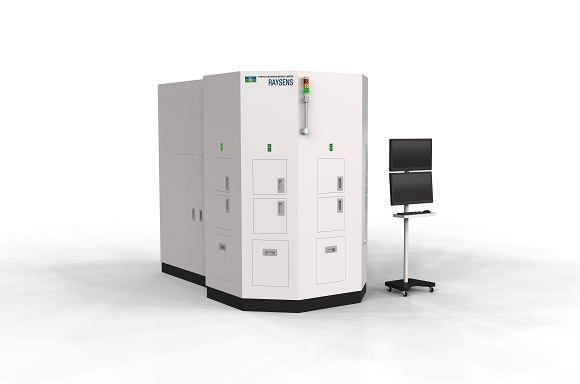
- LT/LN Wafer Defect Inspection System
Products & Services
LT/LN Wafer Defect Inspection System
LT and LN wafers are mainly used for SAW devices in wireless communication terminals like smartphones. These devices act as crucial filters to prevent noise and interference during voice and data communication. With increasing production and size scaling, the demand for SAW devices is expected to rise, highlighting the growing importance of automated appearance inspection. Click here for the Japanease site
- Application
- Target Defects
- Features
- Specification
- Sample Evaluation
- Glossary
- 【Spotlight】Revolutionizing AI Chips
Application
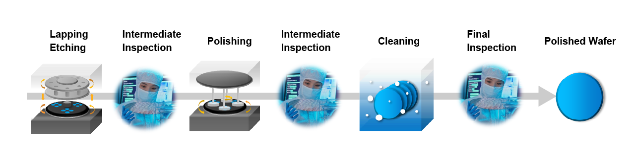
・Final inspection of LT/LN wafers
・Inspection after grinding
・Inspection after polishing
Candidate Introduction Inspection Process
Target Defects
・Surface:Scratch, particles, color unevenness, cracks, chipping, dirt, cleaning marks, polishing marks, grinding marks
・Internal:Pinholes
・Back Surface:Scratch, cracks, dirt
・Edge:Chipping, cracks, dirt
Features
High-Speed, High-Sensitivity Inspection
Dedicated line sensor camera and specialized light source for high-speed scanning and defect extraction of LT/LN wafers up to 200mm. Accurate inspection is possible even on highly transparent wafers without being affected by the inspection stage.
Advanced Defect Classification
Automatic classification of typical defects on the surface and backside of LT/LN wafers.
Inspection of Both Front and Back Sides with a Single Unit
Multi-inspection of front surface, back surface, and edge surface with a single unit.
Optimization of Parameters
Optimization of parameters tailored to the criteria of good wafers to suppress undetected and over-detected target defects.
Color Variation Detection
It is possible to perform selection based on the degree of variation such as color variation and quantification of the variation.
Specification
| Item | Detail |
|---|---|
| Supported Wafer Size | 150mm/200mm |
| Supported Wafers | LT/LN Wafer |
| Inspection Sensitivity | Surface:0.3um< ※PSL on Si wafer Edge:1-10μm Internal:1-10μm |
| Throughput | 30-90 seconds per wafer *Varies depending on inspection requirements. |
| Load Port / Cassette Capacity | Min2 ~ Max4(12inch) Min2~Max 10 (8inch) |
| Other Functions | Aligner, ID reader, GEM-compliant |
Sample Evaluation
For customers who would like to use this inspection system to check surface conditions or defects, it is possible to borrow a sample of the workpiece to be inspected and carry out a preliminary evaluation using a demonstration machine. Please contact us to discuss your requirements.


Glossary
- LT, LN Wafers
- LT and LN wafers are single-crystal oxide wafers, referring to Lithium Tantalate and Lithium Niobate, respectively. These wafers can be grown via the Czochralski method (Cz method) and are suitable for mass production, similar to silicon wafers. Additionally, processing of these wafers can be performed using methods similar to those used for silicon.
- SAW Devices
- SAW devices, short for Surface Acoustic Wave devices, are essential high-frequency filters used in wireless communication terminals such as smartphones. These devices consist of electrodes and reflection patterns formed on piezoelectric crystal substrates. They allow for the selective extraction of electrical signals at specific frequencies.
【Spotlight】Revolutionizing AI Chips
- Glass Core Substrate
- RDL Interposer
- UCIe Explained
- Wafer Grinding Processing
- CFET
- Fusion Bonding
- Collective Die to Wafer Hybrid Bonding
- BSPDN (Backside Power Delivery Network)
- BPR (Buried Power Rail)
- CPO (Co-Packaged Optics)
- Silicon Bridge Technology
- HBM (High Bandwidth Memory)
- an Embedded Component Substrate
- Hybrid Bonding
- PLP Technology
- TSV Technology
- Advanced Package Integration
- 2.5D Integration Technology
Documents
Visual Inspection of Semiconductor Wafers
Contact Us
Please feel free to contact us.
LT/LN Wafer Defect Inspection Equipment
 Contact Us
 Download documents
 Member services