- HOME
- Products & Services
- Inspection
- Silicon Wafer Defect Inspection System
Products & Services
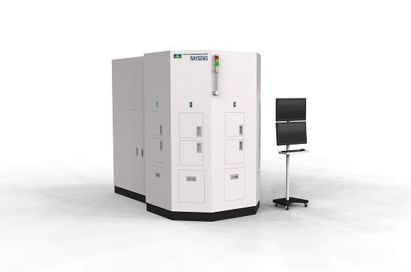
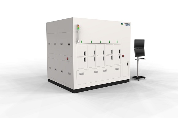
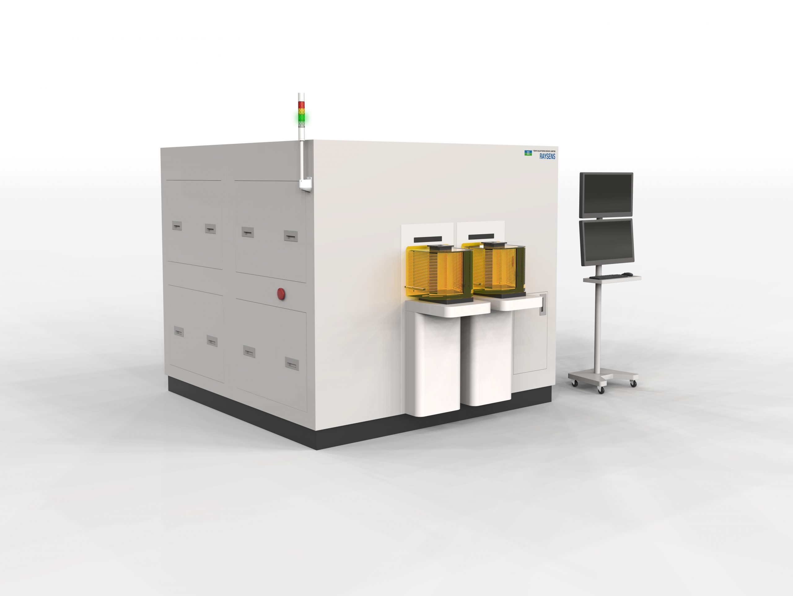
Silicon Wafer Defect Inspection System

The Si wafer defect inspection device uses advanced optical technology to swiftly and sensitively detect defects on both bare and patterned wafers, enabling high-speed, high-sensitivity inspection. With its high throughput, it automates full-scale inspection, replacing traditional visual methods. Click here for the Japanease site
- Application
- Target Defects
- Features
- Specification
- Sample Evaluation
- Glossary
- 【Spotlight】Revolutionizing AI Chips
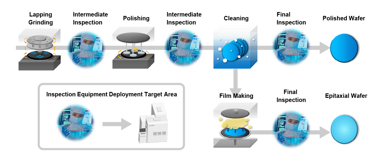
Application
・Final visual inspection of Si wafers and epitaxial wafers
・In-process inspection during Si wafer manufacturing process
・Inspection after lapping and grinding
・Inspection after polishing
Candidate Introduction Inspection Process
Target Defects
・Surface:Scratches, cracks, dimples, chipping, protrusions, particles, dirt, color unevenness, polishing marks, grinding marks
・Epitaxial Surface:Slip, haze
・Internal:Cracks, pinholes (Doping concentration: P+, P++)
・Back Surface:Scratches.
・Edge:Chipping, cracks, dirt
Features
High-Speed, High-Sensitivity Inspection
Detection of minute changes on wafer surfaces is achieved rapidly and with high sensitivity using a specially developed ultra-low noise optical sensor and dedicated lighting.
Particle Risk Reduction
Reduction in inspection time, equipment footprint, and particle risk is achieved through a multi-inspection architecture capable of inspecting defects on both the front and back surfaces as well as the edges with a single unit.
Inspection Time Reduction
Seamless inspection from equipment control to image capture and judgment is realized through dedicated integrated application software.
Traceability
Traceability is achieved by recording all wafer images and detailed data, allowing for:
-Image data and inspection details for each wafer
-History of inspection results for both OK and NG wafers
-Output and storage of inspection data reflecting information such as barcodes and wafer IDs.
Specification
| Item | Detail |
|---|---|
| Supported Wafer Size | 200 / 300mm |
| Supported Wafers | Silicon Wafer, Silicon Epitaxial Wafer |
| Inspection Sensitivity | Surface:0.3um< ※PSL on Si wafer Edge:1-10μm Internal:1-10μm |
| Throughput | 30-90 seconds per wafer *Varies depending on inspection requirements. |
| Load Port / Cassette Capacity | Min2 ~ Max4(12inch) Min2~Max 10 (8inch) |
| Other Functions | Aligner, ID reader, GEM-compliant |
Sample Evaluation
For customers who would like to use this inspection system to check surface conditions or defects, it is possible to borrow a sample of the workpiece to be inspected and carry out a preliminary evaluation using a demonstration machine. Please contact us to discuss your requirements.


Glossary
- Photoluminescence (PL) Method
- The photoluminescence (PL) method is a technique where light is irradiated onto a substance, and the emitted light when excited electrons return to their ground state is observed. Various information can be obtained from the resulting emission spectrum. Since the emission is susceptible to impurities and defects in the material, analyzing this luminescence spectroscopy allows for the non-contact and non-destructive observation of crystal defects in compound semiconductors (such as SiC and GaN).
- Confocal Microscopy
- Confocal microscopy, also known as confocal microscopy, is a type of microscope that focuses light from a point source onto the sample using an objective lens. The reflected light or fluorescence from the sample is then re-imaged through the same objective lens onto a detection point placed optically conjugate to the sample. This method allows for sharper observation of the target object compared to conventional microscopes, enabling detailed information, such as the shape of fine surface defects in semiconductors, to be obtained.
- Scanning Electron Microscope (SEM)
- A scanning electron microscope (SEM) is a device used to observe magnified images of samples using electrons. Electrons have shorter wavelengths compared to light, allowing for the observation of smaller details than conventional optical microscopes. It can observe structures down to a few nanometers and provides images with a deep focal depth. Therefore, it can enlarge the structure of sample surfaces with pronounced irregularities, allowing for the observation of three-dimensional images with a sense similar to that of observing objects with the naked eye.
【Spotlight】Revolutionizing AI Chips
- Glass Core Substrate
- RDL Interposer
- UCIe Explained
- Wafer Grinding Processing
- CFET
- Fusion Bonding
- Collective Die to Wafer Hybrid Bonding
- BSPDN (Backside Power Delivery Network)
- BPR (Buried Power Rail)
- CPO (Co-Packaged Optics)
- Silicon Bridge Technology
- HBM (High Bandwidth Memory)
- an Embedded Component Substrate
- Hybrid Bonding
- PLP Technology
- TSV Technology
- Advanced Package Integration
- 2.5D Integration Technology
Related products

Documents
Visual Inspection of Semiconductor Wafers
Contact Us
Please feel free to contact us.
Silicon Wafer Defect Inspection System
 Contact Us
 Download documents
 Member services