- HOME
- Products & Services
- Inspection
- SiC Wafer Defect Inspection System
Products & Services
SiC Wafer Defect Inspection System
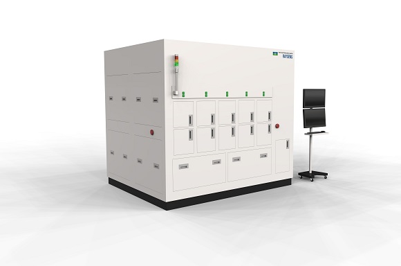
Wide bandgap semiconductors, including SiC, are crucial for power semiconductor control, offering higher efficiency than traditional Si semiconductors and facilitating Green Transformation (GX). As demand surges, especially for EV power control, we’re advancing to 8-inch production. Our enhanced wafer appearance inspection equipment, originally developed for Si, now benefits SiC, aiding in solving customer challenges. Click here for the Japanease site
- Target Defects
- Features
- Specification
- Sample Evaluation
- Glossary
- 【Spotlight】Revolutionizing AI Chips
・SiC wafer, SiC epitaxial wafer final visual inspection
・SiC wafer manufacturing process inspection
・Inspection after lapping and grinding
・Inspection after polishing
Candidate Introduction Inspection Process
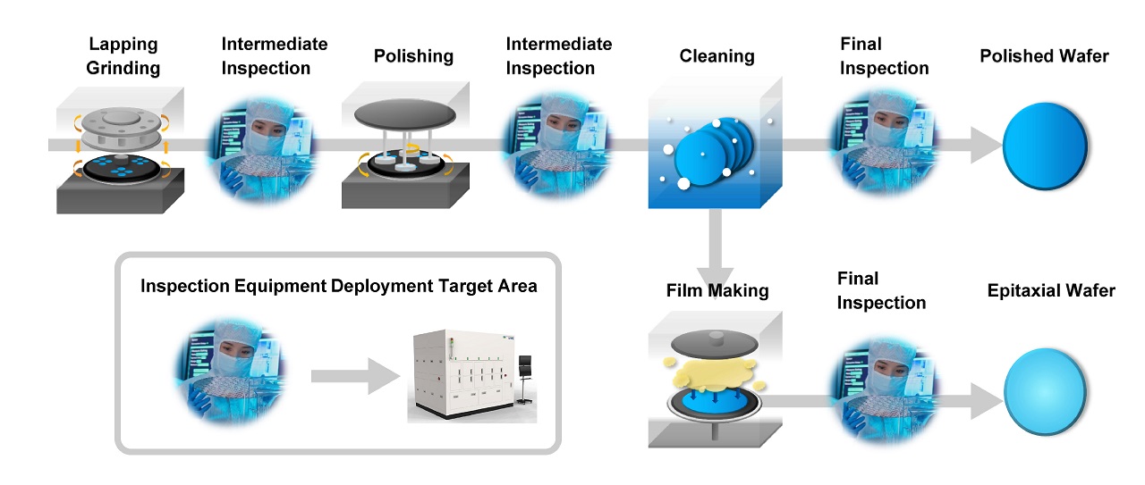
Target Defects
・Surface:Scratches, cracks, dimples, chipping, protrusions, particles, dirt, color unevenness, polishing marks, grinding marks
・Epitaxial Surface:Slip, haze, micro-pipe, bpd, downfall, carrot, step bunching
・Internal:Carbon inclusion, polytype
・Back Surface:Scratches, dirt
・Edge:Chipping, cracks, dirt.
Features
High-Speed, High-Sensitivity Inspection
Whole wafer high-speed scanning and defect extraction using dedicated line sensor cameras specialized for SiC inspection.
Advanced Defect Classification
High-precision defect classification for SiC-specific defects, including Internal defects and surface defects caused by processing.
Color Variation Detection
Detection of surface color variations (polytype defects) that were difficult to detect with conventional inspection equipment.
Inspection of Both Front and Back Sides
Capable of multi-inspection for front surface, back surface, and edge surface with a single unit.
Inspection Time Reduction
Minimization of setup time with specifications for multiple cassettes (up to 10 MAX) and compatibility with 6-inch and 8-inch wafers.
Specification
| Item | Detail |
|---|---|
| Supported Wafer Size | 200 / 300mm |
| Supported Wafers | Silicon Wafer, Silicon Epitaxial Wafer |
| Inspection Sensitivity | Surface:0.3um< ※PSL on Si wafer Edge:1-10μm Internal:1-10μm |
| Throughput | 30-90 seconds per wafer *Varies depending on inspection requirements. |
| Load Port / Cassette Capacity | Min2~Max 10 (6,8 inch cassette compatible) |
| Other Functions | Aligner, ID reader, GEM-compliant |
Sample Evaluation
For customers who would like to use this inspection system to check surface conditions or defects, it is possible to borrow a sample of the workpiece to be inspected and carry out a preliminary evaluation using a demonstration machine. Please contact us to discuss your requirements.


Glossary
- Wide Bandgap Semiconducto
- A semiconductor made from materials with much wider energy band gaps than traditional silicon semiconductors. Due to this wide band gap, wide bandgap semiconductors are suitable for use in high-temperature, high-voltage, and high-frequency environments, enabling efficient power conversion and low energy loss.
- SiC
- Silicon Carbide (SiC) is a semiconductor material composed of silicon and carbon, known for its stability at high temperatures and voltages, as well as its high thermal conductivity. It is being increasingly used in various industries such as power conversion devices, electric vehicle drive systems, and applications requiring high durability. SiC contributes to improving energy efficiency and is considered essential for future technological innovations.
- Power Semiconductor
- Semiconductor devices used for power conversion and control, handling high voltage and large current.
- Green Transformation (GX)
- The process by which economies and societies transition to environmentally friendly and sustainable forms, gaining attention as a means to contribute to Sustainable Development Goals (SDGs).
【Spotlight】Revolutionizing AI Chips
- Glass Core Substrate
- RDL Interposer
- UCIe Explained
- Wafer Grinding Processing
- CFET
- Fusion Bonding
- Collective Die to Wafer Hybrid Bonding
- BSPDN (Backside Power Delivery Network)
- BPR (Buried Power Rail)
- CPO (Co-Packaged Optics)
- Silicon Bridge Technology
- HBM (High Bandwidth Memory)
- an Embedded Component Substrate
- Hybrid Bonding
- PLP Technology
- TSV Technology
- Advanced Package Integration
- 2.5D Integration Technology
Documents
Visual Inspection of Semiconductor Wafers
Contact Us
Please feel free to contact us.
SiC Wafer Defect Inspection System
 Contact Us
 Download documents
 Member services