- HOME
- Products & Services
- Inspection
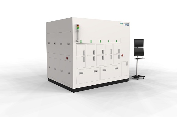
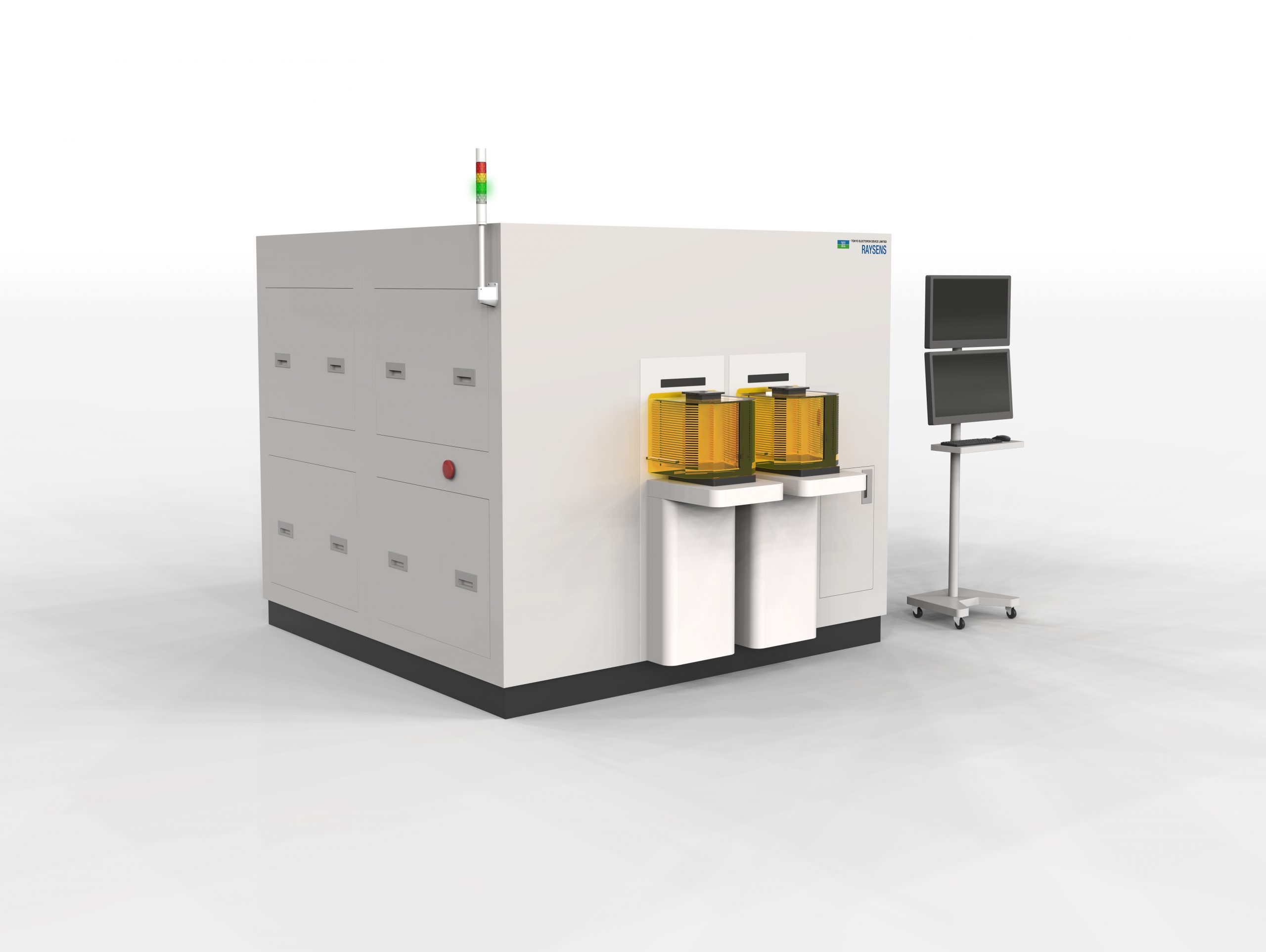
- SiC Latent Defect Inspection System / Bipolar Degradation Simulator “ITS-SCX100”
Products & Services
SiC Latent Defect Inspection System / Bipolar Degradation Simulator “ITS-SCX100”
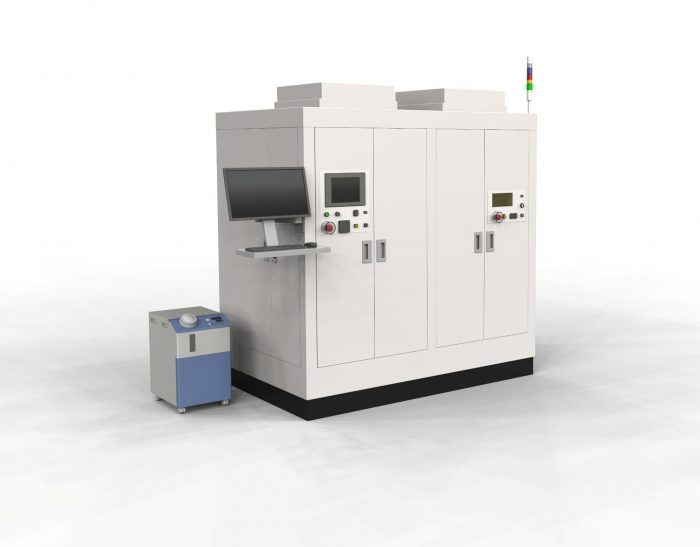
ITS-SCX100 is a novel wafer-level inspection system that accelerates and simulates bipolar degradation in SiC wafers by applying UV irradiation after epitaxial growth.
By reproducing electron–hole recombination phenomena that occur during device current conduction, latent defects can be visualized and evaluated in a significantly shorter time frame.
By non-destructively visualizing stacking faults (SSF) originating from basal plane dislocations (BPD) at the wafer level, the system enables early extraction of latent defects before device fabrication.
This dramatically improves efficiency in mass production ramp-up, process optimization, and material change evaluations, supporting the development of highly reliable SiC devices.
This product is a joint development with ITES Co.,Ltd.
We interviewed ITES Co., Ltd. about the background and development journey of this project. Please see here for the full article.
- Challenges of SiC Bipolar Degradation
- Key Features and Benefits
- Applications of the Defect Inspection System
- Specifications
- Glossary
Challenges of SiC Bipolar Degradation
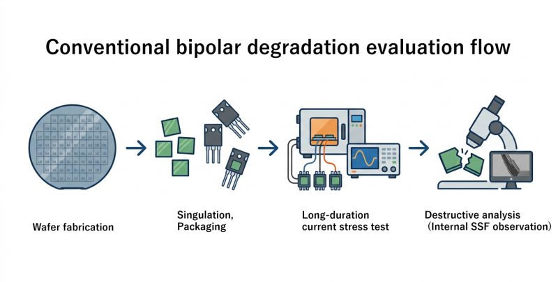
In SiC power devices, bipolar degradation originating from basal plane dislocations (BPDs) formed during SiC substrate growth is a major challenge for long‑term reliability. During current conduction, electron–hole recombination causes these defects to expand laterally along the basal plane, leading to degradation of electrical characteristics and, ultimately, device failure.
At present, the impact of BPDs is mitigated by converting them into threading edge dislocations (TEDs) within the epitaxial layer; however, with prolonged device operation, TEDs can propagate and transform into stacking fault (SSFs), which may eventually become a root cause of failure. Evaluating SSFs requires current stress testing and destructive analysis after chip fabrication, resulting in significant time and cost burdens, while also failing to completely eliminate the risk of defect expansion during actual field use after shipment.
Furthermore, the growing demand for high‑voltage devices with thick epitaxial structures increases the likelihood of SSF generation and propagation. For applications requiring continuous 24/7 operation—such as robotaxis and AI servers—the urgent development of high‑quality SiC devices with minimized bipolar degradation has become essential.
Key Features and Benefits
UV Irradiation Accelerated Evaluation
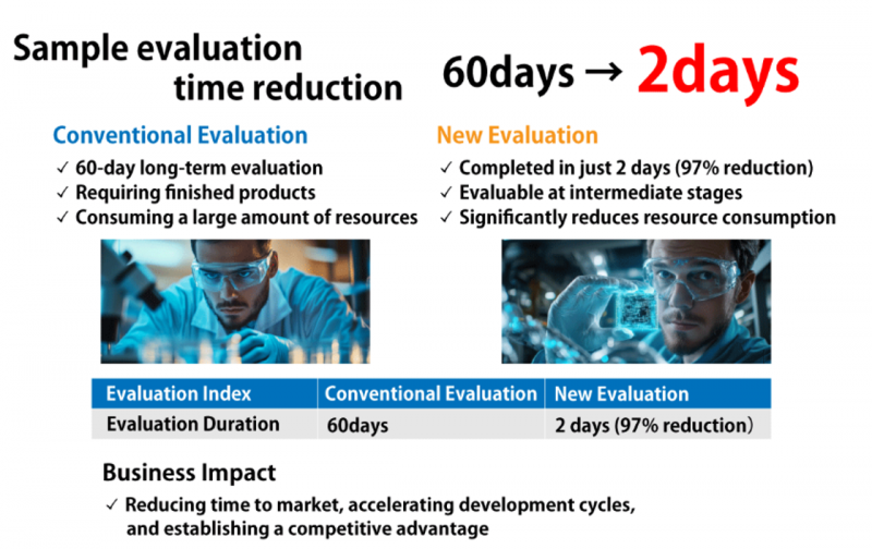
UV laser irradiation simulates carrier recombination under current stress conditions, enabling accelerated reproduction of bipolar degradation at the wafer inspection stage. This replaces conventional long-duration current stress tests and destructive analysis with an in-line wafer inspection process.
UV Irradiation
- Expansion of BPD and stacking faults using UV laser irradiation with proprietary uniform illumination mechanism.
- Alignment mechanism supports both wafer-level and chip-level irradiation.
- Heater stage for UV irradiation reproduces device operating temperature environments.
PL Inspection
- Expanded BPD and stacking faults are observed using an original PL inspection mechanism, enabling analysis of substrate, substrate interface, buffer layer, and drift layer.
- Automatic laser autofocus PL inspection.
- Image processing algorithms classify defect locations (buffer layer, drift layer, substrate interface).
- Defect mapping function with coordinate output.
Applications of the Defect Inspection System
Primary Application Fields
- For Device Manufacturers: Enables evaluation of the impact of stacking faults caused by manufacturing process conditions at each stage of device fabrication.The system supports both wafer‑level and chip‑level inspection.
- For Wafer Manufacturers: Allows wafer‑level verification of the effects of substrate material, epitaxial layer thickness, impurity concentration, and other parameters on defect formation.
- For Device Manufacturers and Wafer Manufacturers: Evaluation of the effects of ion implantation, such as proton and helium implantation, on defect behavior and reliability.
Specifications
Common Specifications
| Item | Details |
|---|---|
| Material | SiC |
| Material size | 150mm/200mm/Chip/Fragment |
| Handling | Manual placement |
| Machine size | Main Unit: (Width) 2060 x (Depth) 1360 x (Height) 2400 (mm) |
| Option | Heat Treatment Function (Defect Shrinkage) |
UV Irradiation
| Item | Details |
|---|---|
| Light Source | UV laser |
| Beam diameter | Φ2-5mm |
| Heater stage | ~200℃ |
| Single Item Sales | Available |
PL inspection
| Item | Details |
|---|---|
| Observation Method | PL Microscope (with Laser Autofocus) |
| Objective Magnification | 5x, 10x |
| Drawing Pixel Size | 4.6um×4.6um |

Visual Inspection of Semiconductor Wafers

Download a Document
The Next Dimension of Semiconductors: Exploring Advanced Packaging
Glossary
Related products


Documents
Contact Us
Please feel free to contact us.
SiC Latent Defect Inspection System / Bipolar Degradation Simulator “ITS-SCX100”
 Contact Us
 Download documents
 Member services