- HOME
- Download documents
Download documents
- For Desgin Engineer
- Evaluation Board & IP Core
- For Process Management
- IT service Inspection
Desgin Engineer / Evaluation Board & IP Core
8K4K Image Evaluation Platform
An evaluation board equipped with Xilinx Kintex UltraScale 115 FPGA. HDMI2. By combining with a video FMC interface card such as 0/DiplayPort1 2/12G-SDI, an 8K4K evaluation environment can be easily constructed.
User Manual
HDMI 2.0 FMC Card
The product is an FMC card for the HDMI2.0 interface composed of Samtec FMC connectors and Texas Instruments’s Retimer LSIs, etc., and each port is guaranteed up to 11.88Gbps. One channel is designed for sink and source. Each channel supports the HDMI2.0 standard. Texas Instruments’s SN65DP159 is used to re-timer the source circuitry.
User Manual
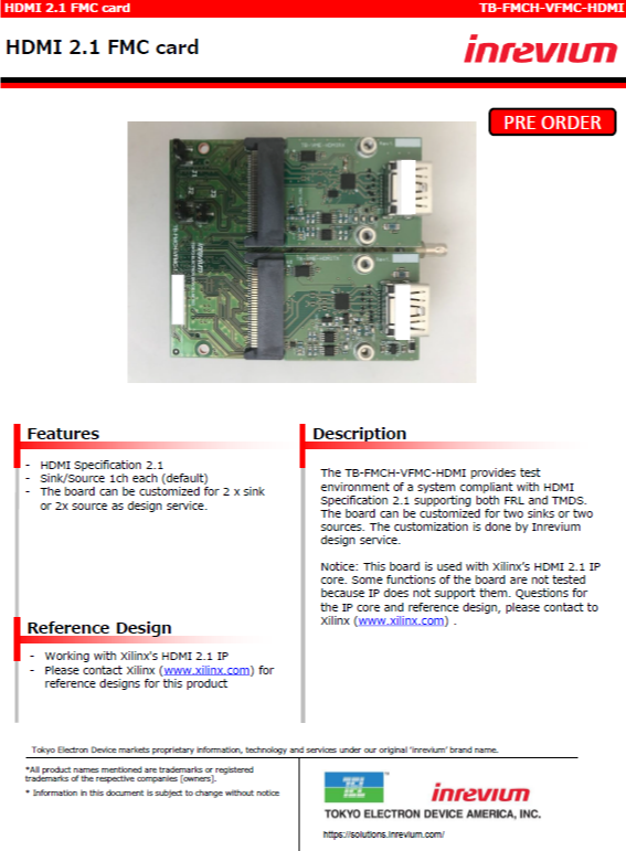
HDMI 2.1 FMC Card
This product is an FMC card ideal for testing HDMI Specification 2 1 compatible with FRL and TMDS. 1ch of Sink, sorce is supported. In addition, we can also consult with our design service for customization of sink/source compatible 2ch each.
Catalog
12G-SDI FMC Card
The 12GSDI FMC card implements a 75-ohm HD-BNC connector with one input, one output, and three inputs and outputs (switchable) between the FMC (HPC) connectors, and two types of on-board clocks (148. 5MHz and 148.3516MHz) are available as reference clocks.
User Manual
DisplayPort 1.4 FMC Card
The DisplayPort 1.4 FMC Card is ideal for the DisplayPort Standard Version1 4 rating environment. It has an IF of 1 channel for sink and source. It uses MegaChips MCDP6000 for the sink side and TI’s SN65DP141 for the source side, and supports 4 lanes of 1.62Gbps, 2. 7Gbps 5. 4Gbps, and 8. 1Gbps. In addition, we can customize the sink/source for each 2ch by our design service.
User Manual
MIPI-DIRECT FMC Card
The MIPI-DIRECT FMC Card provides two separate 4-lane MIPI ports to a pair of 40-pin sockets located in the FMC I/O Window. Each port presents five MIPI lanes (4 data plus clock) with direct, non-translated or isolated connections to FPGA SelectIO pairs provided at the FMC connector.
User Manual
8Lane V-by-One HS LVDS FMC Card
The 8Lane V-by-One HS LVDS card is a board that converts the FMC connector (High-Pin Count) manufactured by Samtec and the FI-R Series connector manufactured by JAE, and supports the V-by-One HS transmission of THine Electronics, Inc. Although JAE-manufactured FI-RE51S-VF is installed, if you want to achieve 16LANE by using the V-by-one HS protocol, you can provide boards that have been changed to FI-RE41S-VF mounting, depending on the configuration of the opposing devices. It is intended for connection to a platform board containing High-Pin Count connectors.
User Manual
Gigabit Ethernet & USB3.0 FMC Card
This FMC card is an evaluation board compatible with Gigabit Ethernet and USB3 0. The Gigabit Etherne is equipped with 2 channels and is ideal for evaluating IEEE802 3. USB30 is a board equipped with a CYUSB3014 chip that supports USB SuperSpeed Peripherals manufactured by Cypress. We assume that the FMC connector from Samtec and the Gigabit Ethernet and USB3.0 TYPE-B connector are used to connect the FMC compatible inrevium evaluation board equipped with the High-Pin Count connector.
User Manual
V-by-One HS IP Core
V-by-One® HS is a standard developed by THine Electronics, Inc. to meet the needs of flat-panel display markets that require higher frame rates and higher resolutions than ever before.
Using the V-by-One HS IP cores for Xilinx FPGA provided by Tokyo Electron Devices, we are able to significantly reduce the number of cables in the device, the cost of developing it, and the time required for developing it.
Data Sheet
User Manual
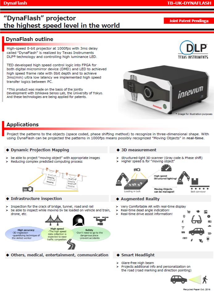
High-speed projector DynaFlash
Using Texas Instruments DLP® DMDs (Digital Micromirror Device) and a high-brightness LED light source, high frame rates are achieved with high-speed control circuitry through proprietary FPGA. In addition, the delay from image generation to projection can be kept to a minimum of 3ms by mounting a circuit for transferring images at high speed on a computer using a unique communication interface. With a frame rate of 1000 fps plus ultra-low delay, we can expect unprecedented technologies to be realized, such as projection mapping to “moving things” as displays in the high-speed vision field and three-dimensional measurement.
Catalog
Process Management / IT service
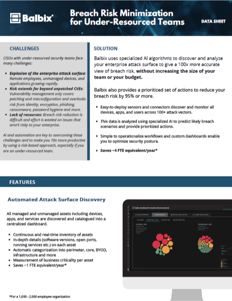
Breach Risk Minimization
With the rapid growth of IoT and BYOD, the number of IT assets managed by companies continues to increase, and the attack methods for these diverse systems are becoming more complex. Balbix uses specialized AI algorithms to discover and analyze the enterprise attack surface to give a 100x more accurate view of breach risk.
Data Sheet
Process Management / Inspection
Silicon Wafer Defect Inspection System
The Si wafer defect inspection device uses advanced optical technology to swiftly and sensitively detect defects on both bare and patterned wafers, enabling high-speed, high-sensitivity inspection. With its high throughput, it automates full-scale inspection, replacing traditional visual methods. Click here for the Japanease site
Visual Inspection of Semiconductor Wafers

SiC Wafer Defect Inspection System
Wide bandgap semiconductors, including SiC, are crucial for power semiconductor control, offering higher efficiency than traditional Si semiconductors and facilitating Green Transformation (GX). As demand surges, especially for EV power control, we’re advancing to 8-inch production. Our enhanced wafer appearance inspection equipment, originally developed for Si, now benefits SiC, aiding in solving customer challenges. Click here for the Japanease site
Visual Inspection of Semiconductor Wafers
LT/LN Wafer Defect Inspection System
LT and LN wafers are mainly used for SAW devices in wireless communication terminals like smartphones. These devices act as crucial filters to prevent noise and interference during voice and data communication. With increasing production and size scaling, the demand for SAW devices is expected to rise, highlighting the growing importance of automated appearance inspection. Click here for the Japanease site
Visual Inspection of Semiconductor Wafers
Glass Wafer Defect Inspection System
Glass is crucial in semiconductor manufacturing due to its flatness, smoothness, and thermal properties similar to silicon. It serves as a support substrate for wafer-level packaging and silicon wafer thinning. Fine-pitched Through-Glass Vias (TGVs) enable high-density TGV formation, enhancing semiconductor performance. Click here for the Japanease site
Visual Inspection of Semiconductor Wafers
Wafer Pattern Defect Inspection Systems
The semiconductor shortage is partly due to supply constraints in legacy nodes, which produce diverse products in small quantities using depreciated equipment. With increasing demand from next-generation devices like IoT, automotive EVs, and XR, bolstering production capacity is crucial. We offer advanced legacy node device inspection equipment, integrating the latest hardware and software inspection technologies, to help address these challenges. Click here for the Japanease site
Visual Inspection of Semiconductor Wafers

Quotation/
Document request/
Technical support etc.
-
 Contact Us
-
 Download documents
-
 Member services