- HOME
- Products & Services
- Inspection
- Glass Wafer Defect Inspection System
Products & Services
Glass Wafer Defect Inspection System
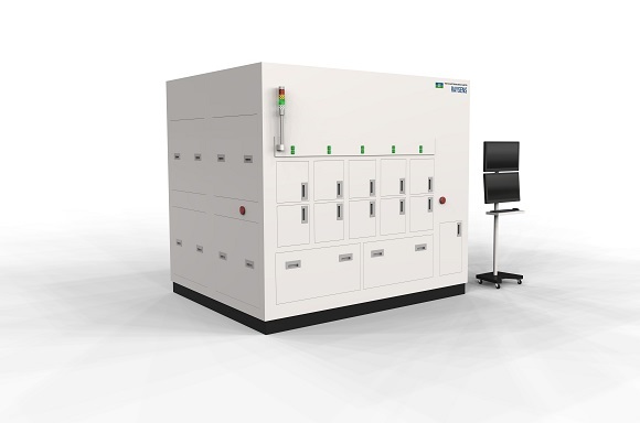
Glass is crucial in semiconductor manufacturing due to its flatness, smoothness, and thermal properties similar to silicon. It serves as a support substrate for wafer-level packaging and silicon wafer thinning. Fine-pitched Through-Glass Vias (TGVs) enable high-density TGV formation, enhancing semiconductor performance. Click here for the Japanease site
- Application
- Target Defects
- Features
- Specification
- Sample Evaluation
- Glossary
- 【Spotlight】Revolutionizing AI Chips
Application
・Visual inspection of glass wafers and glass wafers (recycled)
・Inspection after grinding
・Inspection after polishing
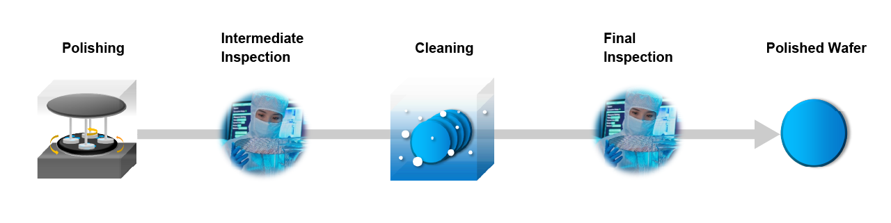
Candidate Introduction Inspection Process
Target Defects
・Surface: Scratch, particles, color unevenness, cracks, chipping, dirt, cleaning marks, polishing marks, grinding marks
・Internal: Bubble
・Back Surface: Scratch, cracks, dirt
・Edge: Chipping, cracks, dirt
Features
High-Speed, High-Sensitivity Inspection
Dedicated line sensor camera and dedicated light source enable high-speed scanning of glass wafers up to 300mm, defect extraction. Accurate inspection is possible without being affected by the inspection stage even for transparent wafers with high light transmittance.
Advanced Defect Classification
Automatically classify typical defects on the surface and backside of glass wafers.
Inspection of Front and Back Sides and Bridge Surfaces with One Unit
Multi-inspection of surface, backside, and edge surfaces is possible with one unit.
Optimization of Parameters
Optimization of parameters according to the criteria of good wafers suppresses undetected and over-detected target defects.
Inspection Time Reduction
Continuous inspection is made possible by multi-cassette specifications, minimizing cassette exchange time.
Specification
| Item | Detail |
|---|---|
| Supported Wafer Size | 200 / 300mm |
| Supported Wafers | Glass Wafer |
| Inspection Sensitivity | Surface:0.3um< ※PSL on Si wafer Edge:1-10μm Internal:1-10μm |
| Throughput | 30-90 seconds per wafer *Varies depending on inspection requirements. |
| Load Port / Cassette Capacity | Min2 ~ Max4(12inch) Min2~Max 10 (8inch) |
| Other Functions | Aligner, ID reader, GEM-compliant |
Sample Evaluation
For customers who would like to use this inspection system to check surface conditions or defects, it is possible to borrow a sample of the workpiece to be inspected and carry out a preliminary evaluation using a demonstration machine. Please contact us to discuss your requirements.


Glossary
- Fan-Out Structure
- The term “fan-out structure” refers to a wiring structure in semiconductor devices where the wiring is spread out in a fan shape around the chip. This structure is formed using wafer processes to create a redistribution layer for pulling out wiring from the terminals of semiconductor chips. It enables chip miniaturization and the supply of devices with a large number of inputs and outputs.
- TGV (Through Glass VIA)
- TGV, or Through Glass VIA, refers to glass substrates with through-holes. With advancements in semiconductor devices such as increased functionality and reduced power consumption, there’s a method of stacking silicon chips in three dimensions. During this process, numerous fine through-holes (VIAs) are required to enable signal transmission between stacked chips vertically. A similar concept is TSV (Through Silicon VIA), where fine holes are processed into silicon substrates.
【Spotlight】Revolutionizing AI Chips
- Glass Core Substrate
- RDL Interposer
- UCIe Explained
- Wafer Grinding Processing
- CFET
- Fusion Bonding
- Collective Die to Wafer Hybrid Bonding
- BSPDN (Backside Power Delivery Network)
- BPR (Buried Power Rail)
- CPO (Co-Packaged Optics)
- Silicon Bridge Technology
- HBM (High Bandwidth Memory)
- an Embedded Component Substrate
- Hybrid Bonding
- PLP Technology
- TSV Technology
- Advanced Package Integration
- 2.5D Integration Technology
Documents
Visual Inspection of Semiconductor Wafers
Contact Us
Please feel free to contact us.
Glass Wafer Defect Inspection System
 Contact Us
 Download documents
 Member services