- HOME
- Products & Services
- Inspection
Products & Services
Inspection
-
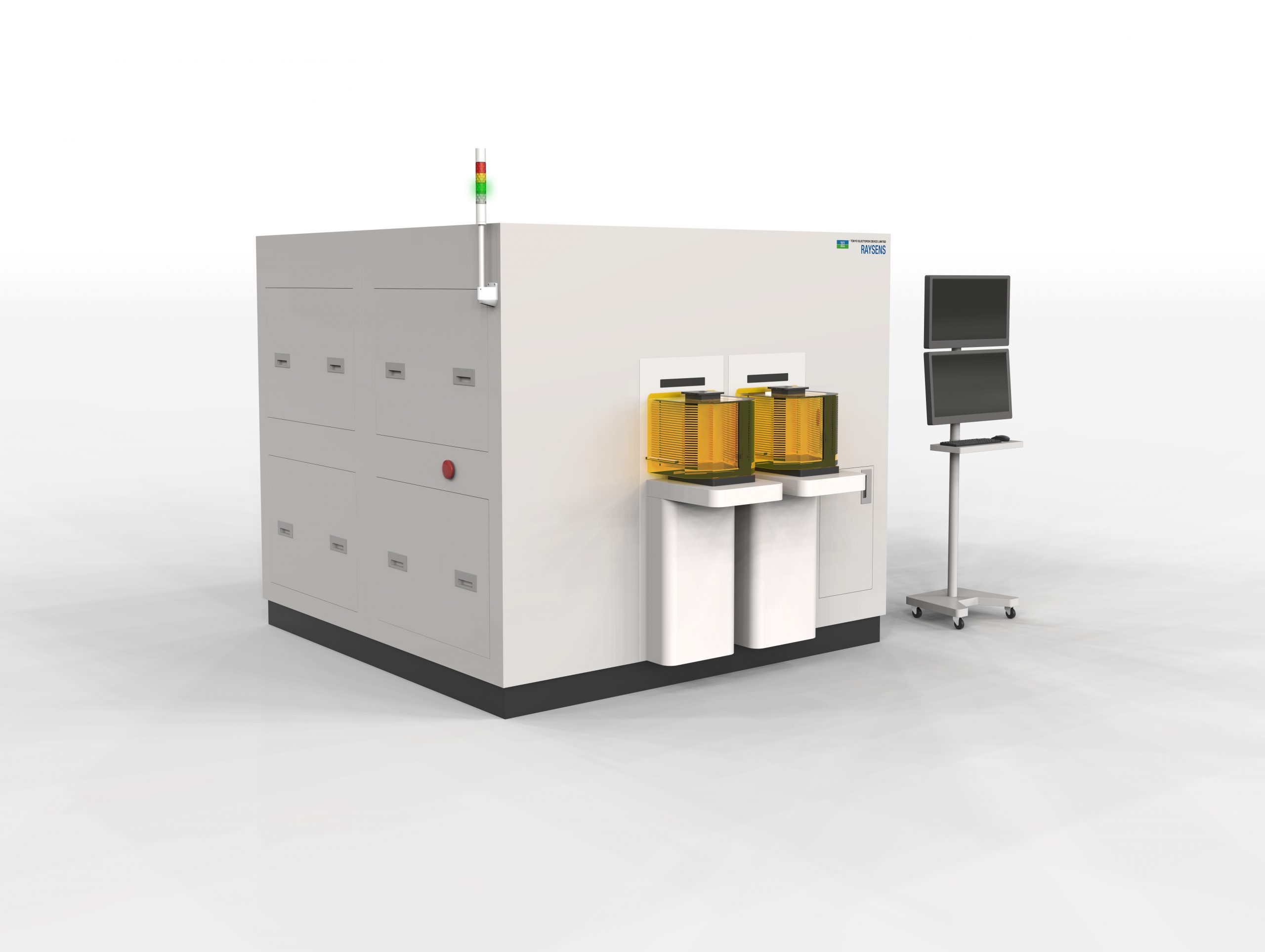
SiC Latent Defect Inspection System / Bipolar Degradation Simulator “ITS-SCX100”
ITS-SCX100 is a novel wafer-level inspection system that accelerates and simulates bipolar degradation in SiC wafers by applying UV irradiation after epitaxial growth. By reproducing electron–hole recombination phenomena that occur during device current conduction, latent defects can be visualized and evaluated in a significantly shorter time frame. By non-destructively visualizing stacking faults (SSF) originating from basal plane dislocations (BPD) at the wafer level, the system enables early extraction of latent defects before device fabrication. This dramatically improves efficiency in mass production ramp-up, process optimization, and material change evaluations, supporting the development of highly reliable SiC devices. This product is jointly developed with ITES Co., Ltd.
-
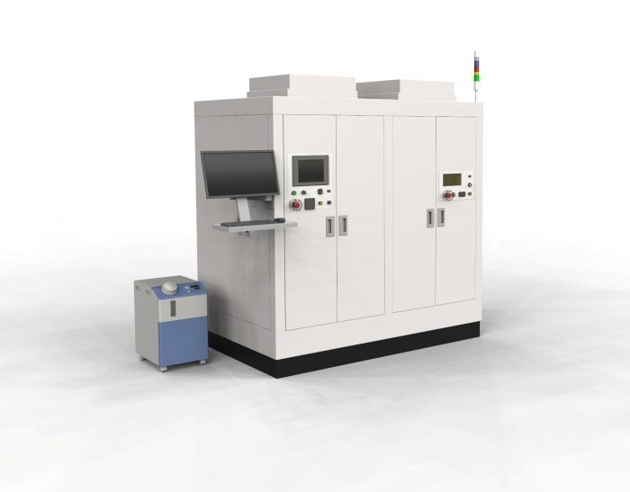
Silicon Wafer Defect Inspection System
The Si wafer defect inspection device uses advanced optical technology to swiftly and sensitively detect defects on both bare and patterned wafers, enabling high-speed, high-sensitivity inspection. With its high throughput, it automates full-scale inspection, replacing traditional visual methods.

-
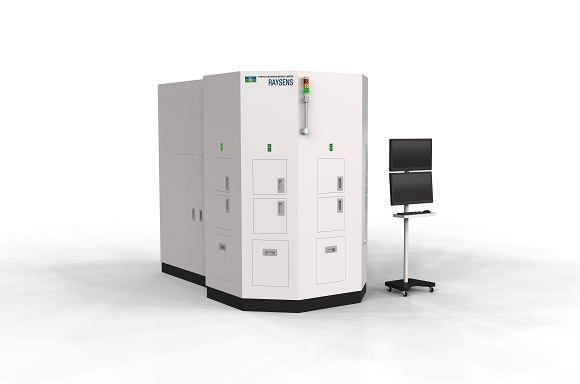
SiC Wafer Defect Inspection System
Wide bandgap semiconductors, including SiC, are crucial for power semiconductor control, offering higher efficiency than traditional Si semiconductors and facilitating Green Transformation (GX). As demand surges, especially for EV power control, we're advancing to 8-inch production. Our enhanced wafer appearance inspection equipment, originally developed for Si, now benefits SiC, aiding in solving customer challenges.

-
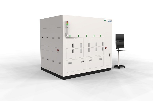
LT/LN Wafer Defect Inspection System
LT and LN wafers are mainly used for SAW devices in wireless communication terminals like smartphones. These devices act as crucial filters to prevent noise and interference during voice and data communication. With increasing production and size scaling, the demand for SAW devices is expected to rise, highlighting the growing importance of automated appearance inspection.
-
Glass Wafer Defect Inspection System
Glass is crucial in semiconductor manufacturing due to its flatness, smoothness, and thermal properties similar to silicon. It serves as a support substrate for wafer-level packaging and silicon wafer thinning. Fine-pitched Through-Glass Vias (TGVs) enable high-density TGV formation, enhancing semiconductor performance.
-
Wafer Pattern Defect Inspection Systems
The semiconductor shortage is partly due to supply constraints in legacy nodes, which produce diverse products in small quantities using depreciated equipment. With increasing demand from next-generation devices like IoT, automotive EVs, and XR, bolstering production capacity is crucial. We offer advanced legacy node device inspection equipment, integrating the latest hardware and software inspection technologies, to help address these challenges.
Contact Us / Download Documents
- Quotation/Document request/Technical support etc.
- Download documents
- Post-purchase technical support
 Contact Us
 Download documents
 Member services