- HOME
- News & Event
- News
- Hear from a Co-Creation Partner
Expose defects with “light”—without applying any current SiC evaluation equipment that reproduces bipolar degradation: the road to development
News & Event
News
2026/04/14
Column
Hear from a Co-Creation Partner
Expose defects with “light”—without applying any current SiC evaluation equipment that reproduces bipolar degradation: the road to development
SiC power semiconductors face an unresolved challenge that is hindering mass production and widespread adoption: “bipolar degradation.” ITES Co., Ltd. (“ITES”) is taking on this issue with an innovative simulation technology that uses light.
The company’s Bipolar Degradation Simulator enables defects to be visualized and evaluated at the wafer stage—without going through device prototyping.
We spoke with President and Representative Director Yasuyuki Igarashi and development leader Takuya Morita about the background to this development, its technical features, and their partnership with Tokyo Electron Device.
Interviewees
ITES Co., Ltd.
President and Representative Director
Yasuyuki Igarashi

ITES Co., Ltd.
Product Development Department, Engineering Section
Staff Engineer
Takuya Morita

- Defects that only surface after 1,000 steps—structural problems with conventional screening methods
- How the Bipolar Degradation Simulator was developed and its four key technical features
- Dramatically shorter evaluation time and earlier detection at the wafer stage
- Moving toward deployment on mass-production lines through collaboration with Tokyo Electron Device
Defects that only surface after 1,000 steps—structural problems with conventional screening methods
—First, could you give us an overview of ITES?
Igarashi: ITES was established in 1993 when the quality assurance organization at IBM Japan’s Yasu facility spun off as an independent company. Around 2000, as IBM moved away from its domestic hardware business, the purpose was to offer the quality assurance and testing technologies we had built up as external services. The company name originally came from the initials of “International Test & Engineering Services,” and today we take the initials of those words and use them as an acronym “ITES”, which is registered as a trademark.
Today our business has two main pillars: failure analysis and materials analysis for semiconductors and electronic components, and the development and manufacture of inspection equipment based on optical technologies. In particular, the latter has earned name recognition in the industry through inspection systems for solar panels, and that know-how led to the development of the SiC (silicon carbide) device inspection system known as the Bipolar Degradation Simulator.
—What challenges do manufacturers working with SiC devices face?
Igarashi: Compared with silicon, SiC performs better in high-temperature and high-voltage environments, and its use is expanding rapidly as a power semiconductor for EVs (electric vehicles) and industrial equipment. However, it also has unique challenges that silicon does not. One of them is “bipolar degradation.”
In SiC crystals, stacking faults can remain hidden from the manufacturing stage. As current continues to flow through the device, these defects expand, increasing electrical resistance and degrading performance. Defects that are rarely an issue in silicon can exist in SiC substrates at densities of hundreds per square centimeter—and they do not necessarily become apparent at the surface when the wafer is newly made.
Even now, more than 20 years after the phenomenon was first identified, the issue has not been fully resolved and has long troubled engineers.
—How do companies address this problem?
Igarashi: Many device manufacturers use a screening method called “burn-in.” They intentionally run a strong current through finished devices to force defects to surface early, and then remove defective products.
However, this approach has major drawbacks. Because power semiconductors consume significant power, it is difficult to process large volumes at once, which drives up cost and time. Moreover, although many defects already exist when the wafer is first received, screening cannot be performed until the very final stage—after completing a device fabrication process that can exceed 1,000 steps. By the time a defect is found, all prior processing has effectively been wasted.
How the Bipolar Degradation Simulator was developed and its four key technical features
—What prompted you to develop the Bipolar Degradation Simulator?
Igarashi: We focused on a phenomenon that the industry has known for about 20 years: simply irradiating the wafer with ultraviolet (UV) light at specific wavelengths can reproduce the same stacking-fault expansion that occurs during current flow. If defects could be expanded by applying light without running any current, we believed it might enable nondestructive evaluation at the wafer stage—and that idea became our starting point.
The idea itself had been proposed in papers by Germany’s Fraunhofer research organization in the 2010s, but it was ultimately not brought into practical use for mass production due to limitations such as insufficient light-source output. Leveraging the photoluminescence (PL) technology we accumulated through developing solar panel inspection systems, we overcame the output barrier by switching the light source from a UV lamp to a UV pulsed laser. After roughly seven years of development, we were able to commercialize it as a production system.
—Could you explain the basic mechanism of the system?
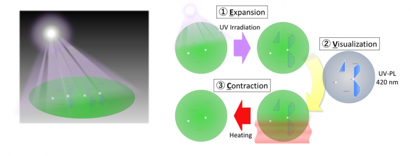
Morita: In a word, it is “a system that performs a burn-in-equivalent evaluation at the wafer stage, without going through device fabrication.” Traditionally, to force defects to surface, it was necessary to fabricate prototype devices and run current through them over several months. With our system, irradiating the wafer with UV light at specific wavelengths induces the same phenomenon. The results are visualized through PL observation, where defects appear in distinctive triangular or bar-like shapes. Wafer manufacturers can use it for pre-shipment inspection, while device manufacturers can apply it to incoming inspection and process-improvement evaluation.
Figure 1. Reproducing bipolar degradation using ITES’s proprietary technology
—From a technical standpoint, what did you focus on most?
Morita: We have presented these features at international conferences related to SiC devices. They are the four points of “uniformity,” “high output,” “correlation,” and “temperature control.”
—Could you walk us through them? First, what do you mean by “uniformity”?
Morita: Bipolar degradation is a very complex phenomenon. If the irradiated light is too weak or uneven, defect expansion may not progress—or it may even recede. That’s why it is essential to design the system so it irradiates the entire sample uniformly at the intended intensity. Many common light sources have poor irradiation uniformity as-is, so we optimized the optical system to achieve uniform irradiation across the sample surface.
—How about the second point, “high output”?
Morita: In EVs and industrial equipment, applications that carry larger currents will continue to increase. To keep up with this shift, higher-intensity UV irradiation is required. The Bipolar Degradation Simulator can apply stress equivalent to a current density of 2,000–3,000 A/cm² and more, reproducing with light a level of stress that is difficult even with burn-in.
Igarashi: At first, we experimented with UV lamps, but we hit the same barrier that led Fraunhofer to abandon commercialization. The output was too low to reproduce large, bar-like-shape defects. As mentioned earlier, switching to a UV pulsed laser enabled a major jump in output. It provides ample performance headroom for future high-power devices as well.
—What does the third point, “correlation,” mean?
Morita: What many device manufacturers want to know is the scale of “how many amps of current does this correspond to?” Because the Bipolar Degradation Simulator applies light, the core of the technology is an equivalence conversion formula that links electrical current to optical intensity. Users input the sample information and the target current value, and the system automatically calculates the corresponding UV irradiation conditions and applies the stress.
—Finally, could you tell us about “temperature control”?
Morita: The expansion of stacking faults depends strongly not only on the applied stress but also on temperature. For example, in EV power modules, it is not uncommon for device temperatures to approach 150°C due to self-heating. In addition to irradiation equivalent to current density, the Bipolar Degradation Simulator includes temperature adjustment functions to reproduce actual operating temperatures, enabling simulations that more faithfully match real use conditions.
Dramatically shorter evaluation time and earlier detection at the wafer stage
—What benefits can be expected from introducing this system?
Morita: The biggest impact is a dramatic reduction in evaluation time. Depending on the case, it can take several months to half a year to fabricate prototype SiC devices, run current through them, and force defects to surface. In contrast, the Bipolar Degradation Simulator eliminates the need for prototyping and can perform an equivalent evaluation in a few days to just a few hours. Put simply, it reduces the evaluation lead time from “months” to “days.”
Igarashi: Another important point is that evaluation can be moved much earlier in the process. As mentioned, many defects already exist at the wafer stage, yet conventional methods could only screen at the final stage after device completion. By applying the Bipolar Degradation Simulator, evaluation becomes possible at incoming wafer inspection, fundamentally reducing waste in downstream manufacturing steps. These benefits have already attracted attention from more than 10 device and wafer manufacturers in Japan and overseas, who are currently conducting trials and evaluations—so we’re seeing a strong response.
Moving toward deployment on mass-production lines through collaboration with Tokyo Electron Device
—How did you come to form a partnership with TED?
Igarashi: When we exhibited at an international SiC conference, a consultant from the European semiconductor industry stopped by our booth and showed strong interest in the Bipolar Degradation Simulator. The consultant also advised that we need an external business partner for commercialization going forward—and introduced us to Tokyo Electron Device.
—How do the two companies work together today, in terms of roles and responsibilities?
Igarashi: We are a small, highly specialized team focused on developing core technologies. On the other hand, we have limited know-how and resources for areas such as defining product specifications and designing the enclosure. Tokyo Electron Device provides broad support in these areas and, by leveraging its sales channels and marketing capabilities across the semiconductor industry, we aim to jointly expand into domestic and global markets.
—What is your roadmap going forward?
Igarashi: We are currently preparing to ship the first unit during fiscal year 2026. First, we will build a track record as a precision evaluation system for R&D (research and development) applications, and within three to four years we aim for full-scale deployment as a screening system on mass-production lines. To scan entire 6-inch and 8-inch wafers within the time required by production lines, another breakthrough will be needed, but we will steadily increase throughput through phased upgrades.
SiC power semiconductors are being adopted at an accelerating pace in a wide range of devices that underpin next-generation social infrastructure. As a result, we have received many comments from professionals at the forefront of the industry saying, “This is exactly the system we’ve been waiting for.” To meet these growing expectations, ITES will work closely with Tokyo Electron Device to accelerate both technology development and market expansion.
Figure 2. Concept image of the new product jointly developed by ITES Co., Ltd. and Tokyo Electron Device, Inc.
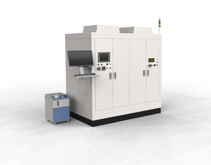
New product: SiC latent defect inspection system / bipolar degradation simulator ITS-SCX100 (concept image)
Combines latent defect expansion via UV irradiation and latent defect observation using a PL microscope in a single system
 Contact Us
 Download documents
 Member services