- HOME
- News & Event
- News
- 【Spotlight】Revolutionizing AI Chips: Glass Core Substrate Explained
News & Event
News
2025/03/18
Column
【Spotlight】Revolutionizing AI Chips: Glass Core Substrate Explained
Among cutting-edge semiconductor technologies, miniaturization and advanced 3D integration play pivotal roles in shaping future semiconductor performance. This article delves into glass core substrate technology.
What is a Glass Core Substrate?
A Glass Core Substrate is a type of IC substrate *¹ used to connect semiconductor chips to PCB boards. IC substrates are classified based on the material used for the core substrate.
Currently, organic resin core substrates dominate high-density integration applications. However, a new type of IC substrate utilizing glass core substrates is under active development, aiming for mass production in the late 2020s.
Advantages of Glass Core Substrates
- High Insulation & Adaptability to High-Speed Communication
- Glass exhibits high insulation properties, minimizing crosstalk *² and electromagnetic noise, making it suitable for high-speed and high-frequency signal transmission.
- Its thermal expansion coefficient closely matches silicon, ensuring stable connections under temperature changes.
- Dimensional Stability & High-Density Integration
- Superior dimensional stability resists temperature and humidity influences, enabling micro-wiring and high-density integration.
- Low signal loss at high frequencies makes it compatible with 5G, 6G communication, and RF devices.
- High Thermal Conductivity & Reliability
- Glass dissipates heat more efficiently than organic resin substrates, making it ideal for high-power devices.
- It also offers high environmental resistance, ensuring stable performance under challenging conditions.
A comparison diagram of organic resin substrates and glass core substrates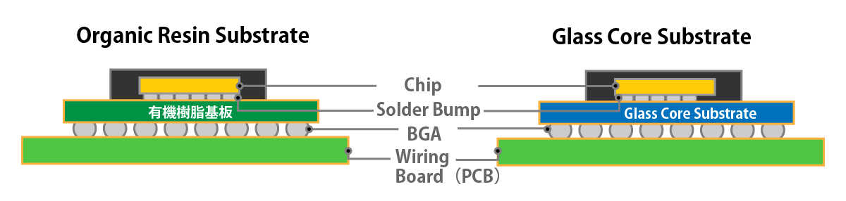
Background of Glass Core Substrate Development
The development of glass core substrates is driven by the increasing demand for larger IC substrates in AI semiconductor applications.
Key Trends
- Chiplet Architectures: AI-focused semiconductors increasingly adopt chiplet structures, requiring larger substrates to accommodate more and larger dies.
- Substrate Size Expansion: Server and data center FC-BGA *³ IC substrates are projected to grow from 56mm×100mm (2022) to 120mm×120mm (2026), with further expansion anticipated.
Challenges with Organic Resin Substrates
Conventional organic resin IC substrates face limitations in dimensional stability, thermal expansion, rigidity, and heat dissipation for next-gen applications.
Advantages of Glass Core Substrates
- Flat surfaces enable direct micro-fabrication using semiconductor front-end processes.
- High-speed communication compatibility contributes to advanced computing evolution.
- Enhanced efficiency in optical-electrical hybrid technologies for reducing AI power consumption.
A comparison diagram of integration using Si interposers and glass core substrates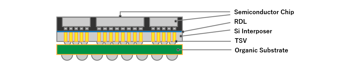
Silicon interposer assembly image
Glass core substrate assembly image (without Si interposer)
Challenges and Prospects of Glass Core Substrates
While glass core substrates present significant potential, several challenges remain:
Challenges
- Micro-Wiring Technology:
- Current technology achieves a minimum L/S (line/space) of 2μm, lagging behind Si interposers (<1μm).
- Further microfabrication advancements are essential for high-density applications.
- TGV Technology Maturity:
- TGV (Through Glass Via) *⁴ requires costly, complex processes like laser or chemical etching, with yield improvement being critical.
- High Manufacturing Costs:
- Although material costs are low, processing costs remain high, posing challenges for large-scale adoption.
Prospects
- High Insulation & High-Frequency Signal Transmission:
- Ideal for next-gen communication technologies (5G/6G) and HPC applications.
- Thermal Expansion Coefficient Compatibility:
- Reliable packaging with minimal distortion under thermal stress.
- Cost Efficiency & Large-Scale Production:
- Large-panel manufacturing reduces per-unit costs, enhancing competitiveness for consumer electronics and IoT.
- Integration with Si Bridges:
- Combining Si bridges with glass core substrates promises high-performance, cost-efficient solutions.
Glass core substrates are poised to become a pivotal technology in next-generation semiconductor packaging, offering solutions to existing challenges in microfabrication, TGV technology, and production costs. With ongoing innovations, these substrates are expected to rival Si interposers, shaping the future of advanced packaging.
Glossary
- IC Substrate: Intermediate layer connecting semiconductor chips to PCB boards, facilitating electrical signal transmission and structural support.
- Crosstalk: Electrical interference between adjacent circuits or transmission paths, potentially degrading signal quality.
- FC-BGA (Flip Chip Ball Grid Array): A packaging technology for high-performance processors and GPUs, offering efficient heat management and electrical characteristics.
- TGV (Through Glass Via): Technology involving vertical holes in glass substrates for signal transmission, enabling advanced packaging and high-density integration.


 Contact Us
 Download documents
 Member services