- HOME
- News & Event
- News
- 【Spotlight】Revolutionizing AI Chips: UCIe Explained
News & Event
News
2025/03/18
Column
【Spotlight】Revolutionizing AI Chips: UCIe Explained
In this series on 3D packaging technologies, we now delve into UCIe, which plays a pivotal role in standardizing chiplet interconnection.
What is UCIe?
UCIe (Universal Chiplet Interconnect Express) refers to a new industry-standard specification designed to enable high-speed interconnection between chiplets. It is also the name of the organization promoting the establishment and adoption of this standard.
UCIe is characterized by participation from a wide range of companies spanning across industries. Notably, competing companies collaborate to advance the standardization process.
Participants include major semiconductor manufacturers like Intel, AMD, Arm, Qualcomm, Samsung, and TSMC. Cloud service providers such as Google Cloud, Microsoft, Meta (Facebook), and Alibaba; IP suppliers like Arm; EDA tool suppliers; and packaging specialists such as ASE are also involved. Moreover, automotive companies, where semiconductor technology is expected to play an increasing role in autonomous driving, are part of the consortium.
This diverse participation underscores UCIe’s broad industry support in driving chiplet standardization and adoption. With contributions from various sectors, UCIe aims to build a highly interoperable and flexible chiplet ecosystem.
As a result of these standardization efforts, UCIe 1.0 was announced in March 2022. This standard suggests that, in the future, chiplets produced by different vendors could be integrated into a single package.
Through this standard, multiple chips can be combined to create high-performance and efficient system-on-chips (SoCs).
Conceptual Diagram of Chiplet Design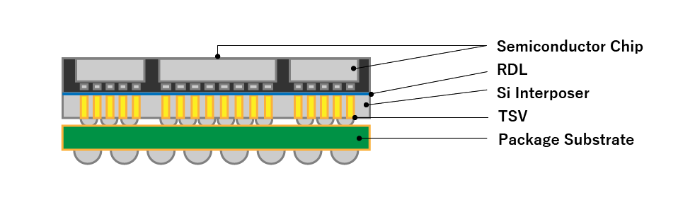
Background of UCIe’s Establishment
The primary motivation for UCIe’s establishment is the growing demand for enhanced computational power driven by AI applications. This has led to a shift from conventional SoC (System on Chip) designs, which integrate various functions onto a single chip, to chiplet technologies that separate these functions into individual chips and reconnect them on a package substrate.
In chiplet technology, the individual dies (chips) do not operate independently; they must be reconnected in 2D or 3D configurations on a package substrate to reproduce SoC functionality.
Consequently, there emerged a need for a standardized approach to efficiently and seamlessly connect dies from different manufacturers and fabrication processes. UCIe addresses this need by standardizing key aspects such as:
- Physical I/O Layer Standardization: Management of electrical signals, clocking, and data rates.
- Protocol Layer Standardization: Support for PCIe, CXL, and custom protocols.
- Form Factor Standardization: Specifications for die size, bump positions, and bump pitches.
- Management Standardization: Standardized software, testing methodologies, and more.
Diagram of Standardization Categories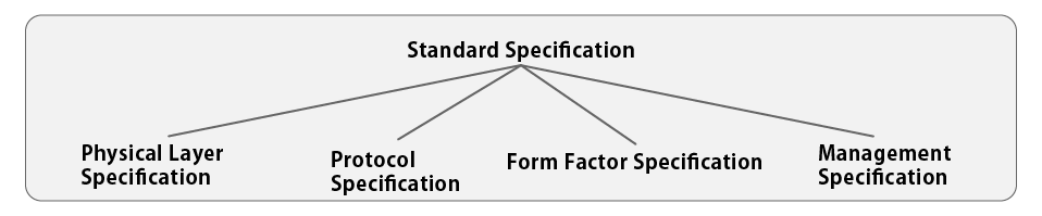
Future Outlook for UCIe
Currently, UCIe’s standards primarily target 2D/2.5D die interconnections on package substrates. However, there is a growing movement to standardize 3D die stacking technologies for even greater performance enhancements.
Moreover, beyond server-focused AI applications, the adoption of edge AI in PCs, smartphones, and automobiles is expected to accelerate. This will necessitate chiplet architectures tailored to these specific devices, along with corresponding standardizations.
The standardization of chiplet interconnections by UCIe is indispensable for accelerating the development of these next-generation devices.
Chiplet technology is poised to provide flexible solutions that cater to market demands across diverse sectors—from the automotive industry to data centers, high-performance computing, and mobile devices.
UCIe is expected to revolutionize design and manufacturing methods in the semiconductor industry, foster a new ecosystem, and drive sustainable technological advancements.
Glossary
- Cloud Service Provider: Companies that provide cloud-based data storage, computing resources, and application services over the internet. Examples include Amazon, Google, and Meta.
- SoC: System-on-Chip, an integrated circuit that consolidates CPU, memory, peripherals, and other components onto a single chip, enabling compact and energy-efficient devices.
- PCIe: Peripheral Component Interconnect Express, a high-speed interface standard for connecting motherboards with peripherals like graphics cards and SSDs.
- CXL: Compute Express Link, an interface standard for low-latency, high-bandwidth data transfer between CPUs and other components like memory and accelerators.
- Form Factor: The physical size, shape, and design specifications of electronic devices or components, ensuring compatibility and interchangeability.


 Contact Us
 Download documents
 Member services