- HOME
- News & Event
- News
- 【Spotlight】Revolutionizing AI Chips: Wafer Grinding Processing Explained
News & Event
News
2025/03/18
Column
【Spotlight】Revolutionizing AI Chips: Wafer Grinding Processing Explained
In this series on 3D integration technologies, this installment provides an overview of wafer grinding processing—a critical process in semiconductor device manufacturing.
What is Wafer Grinding Processing?
Wafer grinding is a type of wafer thinning technology that uses grinding wheels containing diamond abrasives to thin semiconductor wafers. Grinding wheels called cup wheels, which have chip-shaped abrasive bonds arranged in a circular pattern, are used in this process.
Features of Grinding Processing
- Faster Processing: Compared to other wafer thinning technologies such as polishing or etching, grinding is faster because it uses a physical grinding wheel.
- Thickness Control: The use of an in-situ gauge*¹ allows direct measurement of wafer thickness, making it easy to manage thickness.
- Surface Roughness: Grinding leaves surface roughness due to abrasive damage, making it rougher than polishing or etching.
The grinding process is generally divided into coarse grinding and fine grinding.
- Coarse Grinding: Uses coarse-grit wheels to remove 80–90% of the target material quickly.
- Fine Grinding: Uses fine-grit wheels at a slower speed to finish the remaining material.
Due to the damage caused by grinding, it is often combined with polishing processes for damage removal to avoid affecting subsequent processes.
Illustration of Wafer Grinding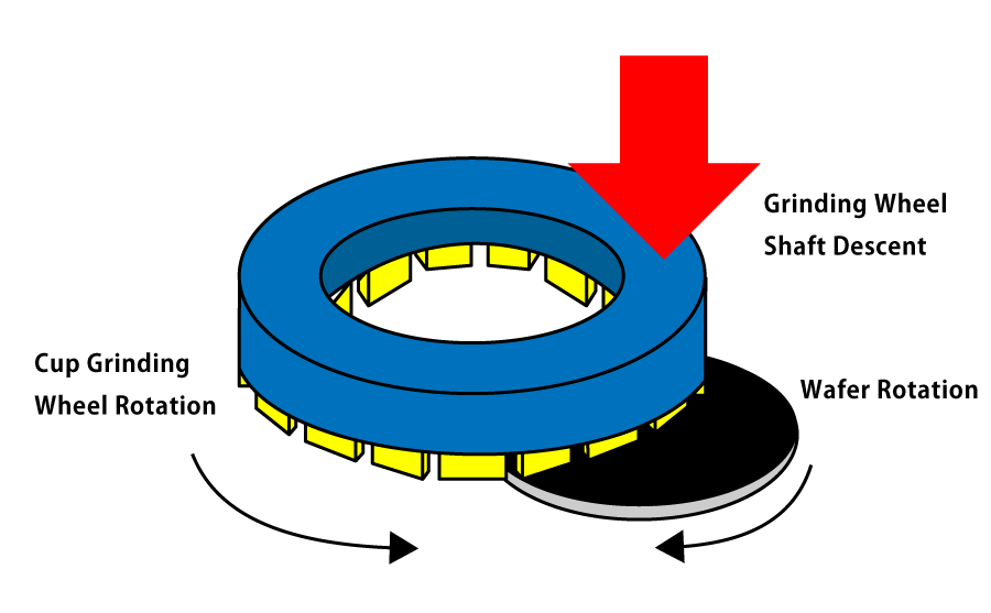
Comparison of Wafer Thinning Methods
| Method | Grinding | Etching | Polishing |
|---|---|---|---|
| Speed | 〇 | △ | × |
| Wafer Damage | ✕ | △ | 〇 |
| Thickness Control | 〇 | △ | × |
Background on the Expansion of Wafer Grinding Processing
Wafer grinding is primarily used for semiconductor wafer thinning and involves two major processes:
- Material Thinning Process
After slicing the wafer from the ingot, the wafer is thinned to meet specified thickness standards. - Back Grinding Process
After the device is fabricated, the wafer’s backside is thinned before it is diced into chips.
Recently, wafer grinding has been rapidly adopted in advanced packaging thinning processes to enhance device performance.
Examples:
- Silicon Interposer Thinning: Used for high-density integration of AI semiconductors.
- HBM (High Bandwidth Memory): Wafer grinding is employed to thin and stack wafers, achieving high-bandwidth memory performance.
- 3D IC Implementation: Wafer thinning and stacking enable better performance, space-saving, and energy efficiency.
In 3D integration, TSV (Through-Silicon Via)*³ wiring is essential, as the wafer thickness directly affects wiring length, impacting performance and power consumption. Therefore, achieving thin and flat wafers for stacking is critical for device performance.
Challenges in Wafer Grinding Processing for Advanced Packaging
Key Challenges
- Equipment Configuration for Pre-Processing
Advanced packaging requires minimal particle contamination and pollution during wafer circuit processes after grinding. - Pushing Thinness Limits
Applications like BSPDN require ultra-thin wafers (e.g., 10 µm), necessitating improvements in wafer thickness control and equipment capabilities. - Simultaneous Grinding of Heterogeneous Materials
For 3D wafer stacking, TSVs need to be exposed for wafer interconnections. This requires grinding both silicon and TSV materials (e.g., copper) simultaneously.
Conclusion
Wafer grinding has been an established technology in wafer thinning, but the emergence of advanced applications like advanced packaging presents new challenges for innovation.
Wafer grinding is more essential than ever for the growth of the semiconductor industry, with high expectations for economic growth and technological advancements.
Glossary
- In-Situ Gauge: A gauge used during the manufacturing process to monitor and measure dimensions or quality in real time.
- HBM (High Bandwidth Memory): Next-generation memory technology that enables high-speed and high-capacity data transfer.
- TSV (Through-Silicon Via): Vertical wiring that penetrates the silicon wafer.


 Contact Us
 Download documents
 Member services