- HOME
- News & Event
- News
- 【Spotlight】Revolutionizing AI Chips: CFET Explained
News & Event
News
2025/03/18
Column
【Spotlight】Revolutionizing AI Chips: CFET Explained
Among advanced semiconductor technologies, along with miniaturization, CFET (Complementary Field-Effect Transistor) is a 3D packaging technology that will significantly influence the future performance of semiconductors. Here is an explanation of CFET.
What is CFET?
CFET (Complementary Field-Effect Transistor) refers to a transistor manufacturing method being considered for adoption in process nodes below 1 nm after 2030.
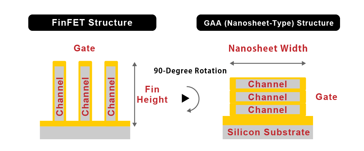
In GAA (Gate-All-Around)¹ transistors, which are under development for mass production in advanced 2 nm processes targeted for 2025, PMOS/NMOS² transistors that compose CMOS standard cells are arranged side by side. However, in CFET, PMOS and NMOS transistors are vertically stacked.
This gives CFET the characteristics of smaller size and higher efficiency. Moreover, CFET operates at low power, making it advantageous in terms of energy efficiency. Particularly in applications such as smartphones and computers, where faster and energy-efficient semiconductor devices are required, CFET is expected to become a crucial technology.
Background of CFET Adoption
The adoption of CFET stems from the necessity to enhance device performance as traditional miniaturization by shrinking gate pitches nears physical limits. Instead, improving device performance requires reducing the overall size of the transistor cell. This has led to efforts to evolve device structures from traditional Planar to FinFET, GAA, and CFET.
To reduce cell size, it is necessary to not only shrink the gate width and increase transistor density but also reduce the metal tracks that run vertically to the gate, thereby decreasing cell height.
While the number of metal tracks has been reduced from over 10 in Planar designs to 5 in FinFET and GAA designs, CFET is being considered as a means to achieve even lower cell heights, essentially eliminating one cell.
Additionally, by vertically stacking PMOS and NMOS, the PN distance*³ is shortened, leading to improved operation speed and energy efficiency.
Evolution of Transistor Structures (Cross-Section View)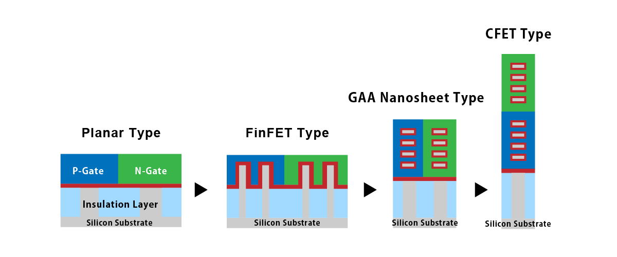
CFET Manufacturing Methods
The manufacturing methods for CFET (Complementary Field-Effect Transistor) primarily fall into two categories: “Monolithic” and “Sequential.” These methods differ in how n-type and p-type transistors are integrated.
In the monolithic CFET manufacturing method, n-type and p-type transistors are integrated simultaneously or through a series of process steps on the same semiconductor substrate. In the sequential CFET manufacturing method, n-type and p-type transistors are created on separate substrates, which are then bonded together to form the device.
The monolithic method has the advantage of lower manufacturing costs compared to the sequential method, but it is more challenging to manufacture as stacking proceeds vertically.
On the other hand, the sequential method simplifies the manufacturing process since it involves bonding separate substrates. However, this method requires two wafers to produce one device, resulting in higher costs.
While further research and development, including manufacturing methods, are necessary for CFET to reach mass production, this innovation is expected to contribute significantly to the evolution of semiconductor devices and the continuation of Moore’s Law by leveraging its unique structural advantages over conventional transistors.
For more details, download the complete guide on semiconductor wafer appearance inspection from here.
Glossary
- GAA (Gate-All-Around): GAA (Gate-All-Around) transistors are a type of semiconductor transistor design where the gate surrounds the semiconductor channel on all sides, achieving high integration density, low power consumption, and high performance.
- PMOS/NMOS: PMOS (P-type Metal-Oxide Semiconductor) and NMOS (N-type Metal-Oxide Semiconductor) are the two basic transistor structures that form CMOS transistors in pairs. PMOS uses P-type semiconductors and turns off with positive voltage. Conversely, NMOS uses N-type semiconductors and turns off with negative voltage.
- PN Distance: The distance separating the p-channel and n-channel transistors.


 Contact Us
 Download documents
 Member services