- HOME
- News & Event
- News
- 【Spotlight】Revolutionizing AI Chips: Collective Die to Wafer Hybrid Bonding Explained
News & Event
News
2025/03/18
Column
【Spotlight】Revolutionizing AI Chips: Collective Die to Wafer Hybrid Bonding Explained
Among advanced semiconductor technologies, 3D integration techniques, along with miniaturization, will significantly impact future semiconductor performance. This section explains Collective Die to Wafer Hybrid Bonding, a key technology in this field.
What is Collective Die to Wafer Hybrid Bonding?
Collective Die to Wafer Hybrid Bonding is a hybrid bonding technique used when vertically stacking two or more semiconductor devices at high density. It is expected to play a critical role in enabling heterogeneous integration ¹, which is considered a key semiconductor technology of the future.
Traditionally, hybrid bonding technologies have employed two methods:
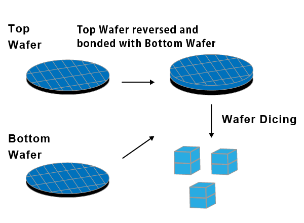
- Wafer-to-Wafer bonding, which bonds wafers together in bulk, offering high productivity but presenting yield issues due to high alignment precision requirements.
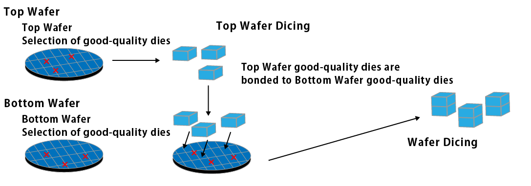
- Die-to-Wafer bonding, which directly bonds individual good die to a wafer, achieving higher yield and alignment precision but at the cost of reduced productivity compared to wafer-to-wafer bonding.
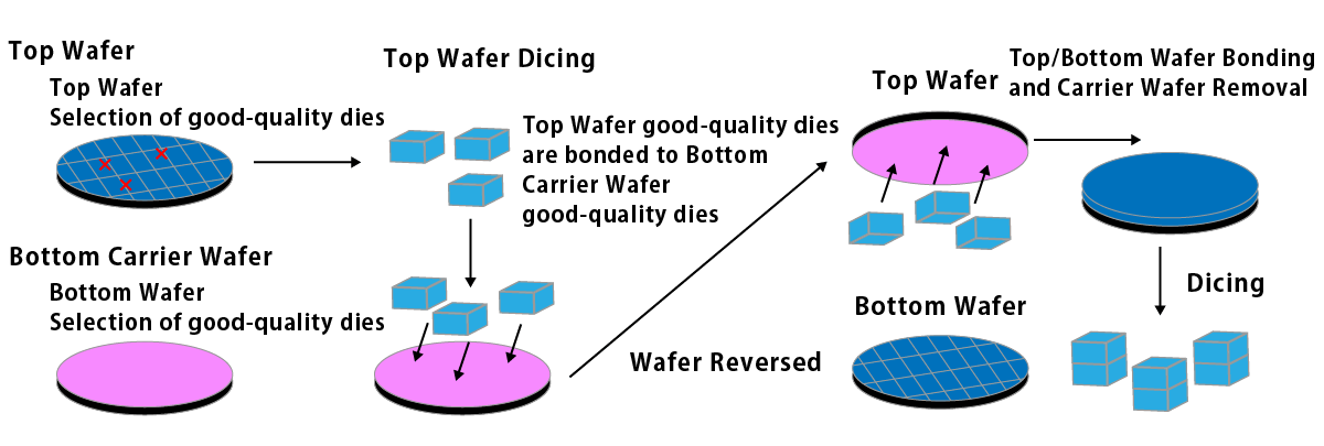
Collective Die to Wafer Hybrid Bonding resolves these issues by first bonding good dies onto a carrier wafer and then collectively bonding them. This approach addresses productivity and yield challenges in traditional hybrid bonding methods.
Wafer-to-Wafer Stacking
Die-to-Wafer Stacking
Collective Die-to-Wafer Stacking
Background for Adopting Collective Die to Wafer Hybrid Bonding
The background for adopting Collective Die to Wafer Hybrid Bonding is the increasing production of heterogeneous chip-connected devices, such as chiplets ², for AI applications. These require bonding technologies capable of high precision and productivity.
Advantages of Adopting Collective Die to Wafer Hybrid Bonding:
- Meeting Demand for High-Density Integration
As devices become smaller and more advanced, demand for high-density chip integration increases. This technology supports the integration of multiple functionalities in a limited space. - Improving Manufacturing Efficiency
The ability to bond multiple dies collectively improves throughput compared to traditional die-to-wafer methods, enhancing production efficiency and reducing costs. - Accommodating Diverse Chips
It enables the integration of different types of chips (e.g., memory, logic, sensors) onto a single wafer, enhancing functionality in devices like smartphones and IoT devices. - Enhancing System Performance
Shortened die-to-die distances improve signal transmission speeds and energy efficiency, particularly crucial for high-performance computing and data center applications.
Advances in precise positioning, bonding, and inspection technologies have made Collective Die to Wafer Hybrid Bonding a feasible and reliable option.
Challenges and Prospects of Collective Die to Wafer Hybrid Bonding
Although Collective Die to Wafer Hybrid Bonding represents significant progress in the semiconductor industry, it faces several challenges:
- Alignment and Precision
Maintaining high alignment precision, particularly for small die sizes, is difficult. Misalignment can lead to performance degradation and defects. - Consistency in Bonding Quality
Ensuring uniform bonding quality when bonding multiple dies simultaneously is technically challenging. Variability can impact reliability. - Thermal Management
Differences in thermal expansion rates between materials may cause issues during bonding or operation. - Scaling and Cost
Initial capital investment is high, and scaling the process incurs costs, making mass production challenging. - Defect Management and Inspection
Defects in individual dies can affect the entire assembly, requiring stringent quality inspections.
Despite these challenges, Collective Die to Wafer Hybrid Bonding is expected to play an essential role in the semiconductor industry due to its advanced integration capabilities and efficiency. Overcoming these obstacles and further maturing the technology will expand its application scope.
Glossary
- Heterogeneous Integration: The technology of integrating different materials, processes, and devices into a single system. This approach combines components with varying functionalities and characteristics to create systems with enhanced performance and functionality that cannot be achieved with a single material or process.
- Chiplet: A method of dividing multi-functional devices, traditionally manufactured as a monolithic chip, into smaller functional chips (chiplets) and then re-integrating them horizontally or vertically on a separate substrate to create a module with the same functionality as the original chip.


 Contact Us
 Download documents
 Member services