- HOME
- News & Event
- News
- 【Spotlight】Revolutionizing AI Chips: BSPDN (Backside Power Delivery Network) Explained
News & Event
News
2025/03/18
Column
【Spotlight】Revolutionizing AI Chips: BSPDN (Backside Power Delivery Network) Explained
Among advanced semiconductor technologies, along with miniaturization, BSPDN (Backside Power Delivery Network) is a 3D packaging technology that will significantly influence the future performance of semiconductors. Here is an explanation of BSPDN.
What is BSPDN (Backside Power Delivery Network)?
BSPDN (Backside Power Delivery Network) is a semiconductor technology aimed at improving the efficiency of power supply to semiconductor chips.
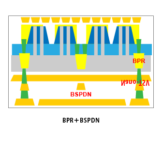
This involves moving the entire power delivery network, which was traditionally located in the upper layers of transistors, to the backside of the silicon wafer. This separation of the power delivery network and the signal network improves power delivery efficiency and reduces interference between different networks.
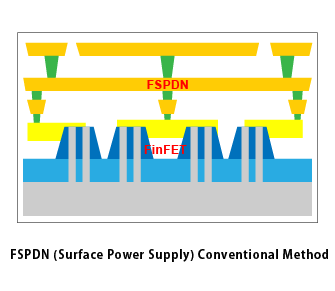
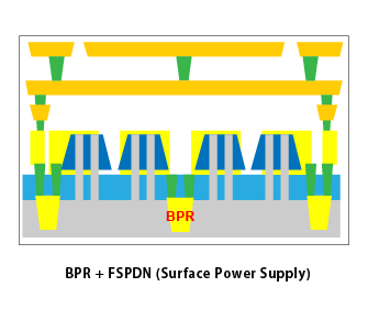
The implementation process begins with a technique called BPR (Buried Power Rail)*¹, embedding power lines and ground lines beneath the transistor. Then, BSPDN is formed on the backside of the BPR to supply power to the BPR, which in turn supplies power to the transistor. Power supply between BSPDN and BPR is carried out via vertical vias.
By combining BPR and BSPDN, power can be delivered to transistors over the shortest distance, improving the efficiency of power transmission and contributing to the overall performance of the chip. The separation of the power supply network and the signal network significantly reduces interference between the two, contributing to improved signal quality.
Additionally, utilizing the backside of the wafer, which was not previously used, allows for the integration of more transistors and circuits on the front side, enabling the design of smaller, higher-performance semiconductor devices.
Background of BSPDN Adoption
The background of BSPDN adoption includes addressing the challenges of providing stable power supply from the upper layers of transistors due to advancements in miniaturization driven by Moore’s Law*².
Specifically, as miniaturization progresses, the number of transistors within the same area increases. Consequently, the total number of interconnections stacked between transistors increases, increasing the distance from the power supply points to the transistors, which causes issues such as IR drop*³. Longer wiring distances increase wiring resistance, contributing to heat generation.
Additionally, with the conventional surface power supply, the signal supply network and the power supply network exist in the same space, causing potential signal interference and delays, negatively impacting the system.
Moreover, there is a space utilization issue. Compared to signal networks, power delivery networks occupy a larger width of wiring, taking up significant space in the same area and not fully benefiting from the system shrinkage enabled by signal line miniaturization under Moore’s Law.
BSPDN is expected to break the limitations of traditional power supply methods, enabling high performance and low power consumption.
Challenges and Prospects of BSPDN
While BSPDN offers numerous benefits for enhancing the functionality of semiconductor devices, it requires designs and manufacturing processes that differ from conventional methods. Specifically, there is the need for nano-TSV technology to connect BSPDN to BPR after forming BPR.
The current TSV diameter used in Si interposers is approximately 10 μm, whereas nano-TSVs require a diameter of about 100 nm, necessitating extremely fine processing. The Si used to form TSVs requires support for thinning, involving bonding to another substrate, and subsequent thinning from a thickness of 775 μm to a few hundred nanometers.
The same level of in-plane uniformity is also required. For thinning, processes such as grinding, etching, and CMP must be combined. After thinning, wiring layers need to be formed during the BEOL process*⁴.
Thus, the need arises for continuous implementation of processes previously uncommon in front-end manufacturing, such as grinding and bonding, alongside traditional pre-wiring formation processes, introducing new technical challenges.
Nevertheless, these challenges also promote new technological advancements and innovation within the semiconductor industry, creating opportunities for new applications and markets. BSPDN represents significant progress in semiconductor technology, and while its implementation poses challenges, the advantages and potential it offers are immense.
For instance, BSPDN is being considered for devices used in high-performance computer systems and server-oriented devices represented by AI. These devices need to maximize computing power while minimizing power consumption.
The adoption of BSPDN is a crucial step to meet these technical and market demands, significantly contributing to the improvement of semiconductor device performance and power efficiency.
Comparison Image of Conventional Structures and BSPDN (Cross-Section)
For more details, download the complete guide on semiconductor wafer appearance inspection from here.
Glossary
- BPR (Buried Power Rail): BPR (Buried Power Rail) refers to the manufacturing technology that places power rails, traditionally located on the front side of transistors, on the backside of transistors.
- Moore’s Law: Moore’s Law predicts that the number of transistors on an integrated circuit will double approximately every two years.
- IR Drop: IR drop refers to the voltage drop caused by current flowing through resistance.
- BEOL Process: The BEOL (Back-End-of-Line) process is the latter stage of semiconductor manufacturing, where circuit wiring, insulation layers, and other interconnections are formed.


 Contact Us
 Download documents
 Member services