- HOME
- News & Event
- News
- 【Spotlight】Revolutionizing AI Chips: BPR (Buried Power Rail) Explained
News & Event
News
2025/03/18
Column
【Spotlight】Revolutionizing AI Chips: BPR (Buried Power Rail) Explained
Among advanced semiconductor technologies, miniaturization and 3D integration significantly impact future semiconductor performance. This article explains the BPR (Buried Power Rail) technology, one of the core 3D integration technologies.
What is BPR (Buried Power Rail)?
BPR (Buried Power Rail) is a technology that embeds power and ground lines (Power Rail), previously placed on the upper layers of devices, into the substrate or insulating layers beneath the device. This approach redistributes power from external sources like PCBs or package substrates across the device.
Currently, it is mainly adopted in advanced nodes of 5nm and below. By employing this technology, devices achieve further miniaturization, stable power supply, and maximized performance in advanced devices.
Specific Benefits:
- Reduction of Wiring: Power and ground lines are relocated to the device’s lower layers, leaving only signal lines on the upper layers, reducing the overall number of metal tracks (Metal Track¹).
- Miniaturization: By reducing the number of upper-layer wires, the physical size of devices can be minimized (Cell Height² reduction).
- Lower Electrical Resistance: The power/ground lines in BPR can achieve a high aspect ratio (height/width), which reduces electrical resistance and contributes to mitigating IR drops (IR Drop³).
Background of BPR Adoption
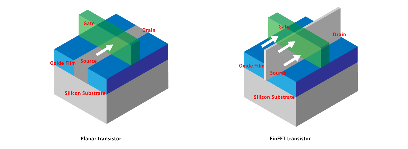
Traditional planar MOS transistors faced difficulties in miniaturization due to short channel effects (Short Channel Effect⁴) at 28nm–22nm nodes. From the 16/14nm node onward, FinFET transistors with a 3D structure were introduced, enabling better control of short channels.
Challenges with FinFET:
- Despite the improvements of FinFET, gate length could no longer shrink as before, prompting the need to reduce Cell Height for further miniaturization.
Solution:
- BPR relocates power and ground lines to the device’s lower layers, reducing the height of the standard cells (Cell Height) while maintaining performance.
This background has driven the adoption of BPR in advanced nodes.
Comparison Between Conventional Planar and FinFET Structures
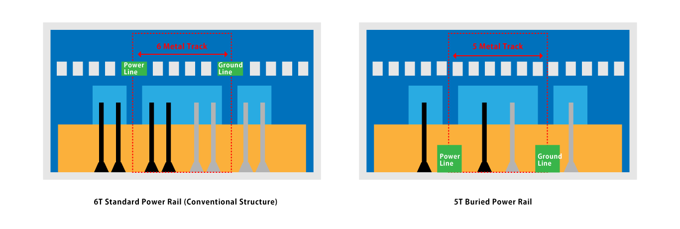
Comparison Between Conventional and BPR Structures (Cross-Section)
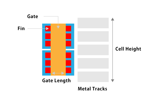
FinFET Cell Structure (Top View)
Challenges and Outlook for BPR
Challenges:
- Increased Manufacturing Complexity:
- Implementing BPR requires additional or modified manufacturing processes, increasing production complexity.
- Thermal Issues:
- Embedded power lines can hinder heat dissipation, potentially impacting device thermal behavior.
- Integration Challenges:
- Integrating BPR with existing manufacturing processes and design flows presents challenges.
Future Prospects:
- Advanced Materials:
- Developing materials with superior thermal and electrical conductivity.
- Process Innovation:
- Combining technologies like BSPDN (Backside Power Delivery Network) and Nano-TSV to enhance semiconductor performance further.
BPR is expected to play a key role in improving both performance and manufacturing efficiency, driving the next generation of semiconductor devices.
Glossary
- Metal Track: Parallel metal lines in an IC for electrical connections.
- Cell Height: The physical height of a standard cell, defined by the number of metal tracks and their pitch.
- IR Drop: Voltage drop caused by resistance in power/ground lines, which can affect chip performance.
- Short Channel Effect: Unintended effects in MOSFETs as gate length shortens, impacting transistor performance.
- Standard Cell: A block of transistors with a specific logic function, standardized in height and width.
- BSPDN: Technology for delivering power from the backside of the IC.
- Nano-TSV: Ultra-fine through-silicon vias for advanced vertical connections.


 Contact Us
 Download documents
 Member services