- HOME
- News & Event
- News
- 【Spotlight】Revolutionizing AI Chips: Silicon Bridge Technology Explained
News & Event
News
2025/03/18
Column
【Spotlight】Revolutionizing AI Chips: Silicon Bridge Technology Explained
Among advanced semiconductor technologies, 3D integration significantly impacts future semiconductor performance alongside miniaturization. This article explains Silicon Bridge Technology, a key component of 3D integration.
What is Silicon Bridge Technology?
Silicon Bridge Technology embeds a silicon substrate (silicon bridge) for interconnection within a semiconductor package, enabling high-density mounting and interconnection of silicon chips on the package.
By forming fine and dense wiring on the surface of the silicon bridge, adjacent silicon chips can be mounted in close proximity on the package substrate.
Key Features of Silicon Bridge Technology
- Heterogeneous Integration:
Silicon bridges connect chips manufactured using different process nodes within the same package. Using fine vias (vertical electrical connections), the physical distance between chips is minimized, enabling direct and short interconnections. - Flexible Chip Placement:
Chips can be placed in any position on the package and connected using silicon bridges as needed. This optimizes package space and minimizes inter-chip distances. - Optimized Manufacturing for Performance and Cost:
For example, high-speed computing chips can be fabricated with advanced process nodes, while large-capacity memory chips in the same package can be fabricated with mature process nodes. This approach maximizes overall performance and energy efficiency.
Detailed structure of a silicon bridge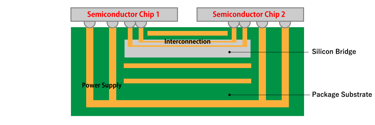
Comparison Between Silicon Bridge and Silicon Interposer Technologies
Advantages of Silicon Bridge Technology
- Lower Cost:
Silicon bridges require less silicon area compared to silicon interposers, reducing costs. Additionally, as the number of silicon dies increases, more silicon bridges can be added without significant cost increases. - No TSV Requirement:
Unlike silicon interposers, silicon bridges deliver power through the package substrate, eliminating the need for TSV (Through-Silicon Via) formation, which further reduces costs.
Limitations of Silicon Bridge Technology
- Limited Chip Connectivity:
Connections are limited to relatively few chips due to the physical size and shape constraints of the silicon bridge. - Design Complexity for Large Packages:
Connecting many chips in a large package requires more silicon bridges, increasing design complexity and manufacturing costs, thus reducing cost benefits. - Signal Transmission Issues:
Longer distances between chips connected via large silicon bridges may lead to signal propagation delays and degradation, especially for high-frequency signals.
Currently, for applications requiring dense interconnection of many chips in a package, technologies like silicon interposers are still necessary.
Structural comparison of silicon bridges and silicon interposers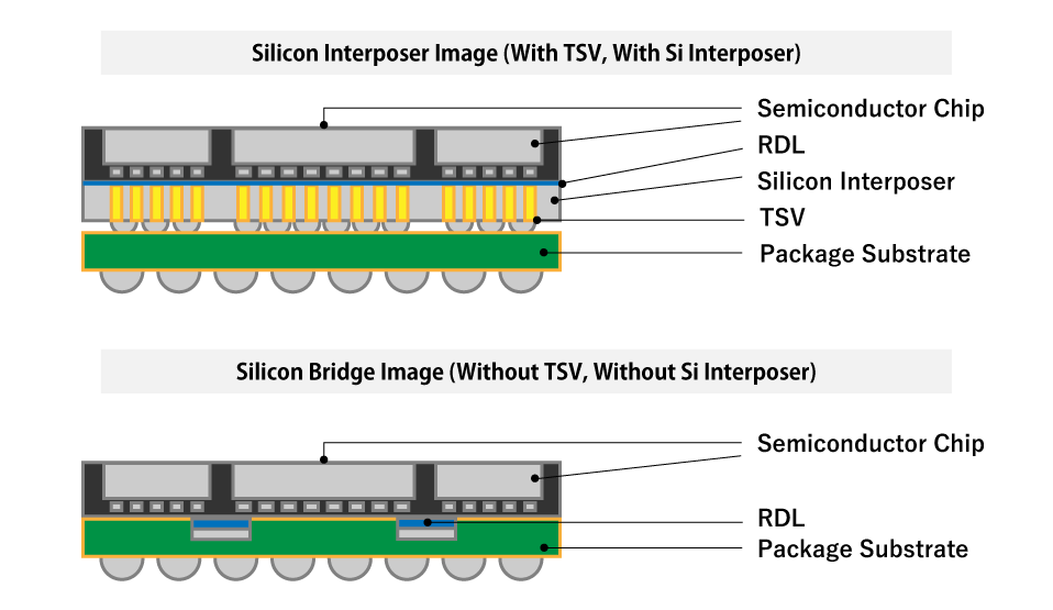
Challenges and Future Prospects of Silicon Bridge Technology
Challenges
- Scalability for Large Chip Arrays:
Silicon Bridge Technology is optimized for connecting relatively few chips. For large-scale integration, silicon interposers or other packaging technologies may be more suitable. - Physical Limitations on Chip Placement:
The physical position and distance between chips connected via silicon bridges are constrained. Longer distances can cause signal propagation delays and impact signal quality, especially in high-performance applications. - Complex Manufacturing Processes:
Silicon Bridge Technology requires high precision and manufacturing control, posing challenges for cost-effective and reliable mass production.
Future Prospects
Despite these challenges, Silicon Bridge Technology is expected to evolve alongside advancements in packaging technologies. Potential developments include:
- Higher-density chip interconnections.
- Broader compatibility with diverse process nodes.
- Improved manufacturing processes for better cost efficiency and reliability.
Combining Silicon Bridge Technology with 3D packaging could further enhance performance and functionality, making it a crucial part of future semiconductor advancements.
While currently used in high-end semiconductor applications, Silicon Bridge Technology is expected to expand its influence and adoption in both specialized and general-purpose applications as technological progress and market demands evolve.
Glossary
- Heterogeneous Packaging: A packaging technology that integrates different types or functions of semiconductor chips within a single package. This approach allows each chip to be manufactured using its optimal process node.
- Process Node: A measure of semiconductor manufacturing precision, indicating transistor size and density. Smaller process nodes enable higher performance and better energy efficiency. Examples include 90 nm, 45 nm, 14 nm, 7 nm, 5 nm, and 3 nm.


 Contact Us
 Download documents
 Member services