- HOME
- News & Event
- News
- 【Spotlight】Revolutionizing AI Chips: HBM (High Bandwidth Memory) Explained
News & Event
News
2025/03/18
Column
【Spotlight】Revolutionizing AI Chips: HBM (High Bandwidth Memory) Explained
Among advanced semiconductor technologies, 3D integration plays a crucial role in shaping the future performance of semiconductors alongside miniaturization. This article explains HBM (High Bandwidth Memory), a core component of 3D integration.
What is HBM (High Bandwidth Memory)?
HBM (High Bandwidth Memory) is a type of DRAM designed for extremely high data transfer rates, or bandwidth.
In memory systems, the circuit connecting the memory to the processor for data exchange is called a bus, and the number of data signals transmitted through the bus per second is referred to as bandwidth. Higher bandwidth indicates faster data processing. Bandwidth is determined by the transmission speed per signal line × number of bus lines.
For instance, DDR3 (Double Data Rate) DRAM with a transmission speed of 1,600 Mbps and 32 bus lines achieves a bandwidth of 6.4 GB/s (51,200 Mbps).
In contrast, HBM2, with a transmission speed of 2 Gbps and 1,024 bus lines, delivers a bandwidth of 254 GB/s, achieving both high transmission speed and significantly more bus lines.
Why Does HBM Achieve High Bandwidth?
HBM achieves its remarkable performance through:
- High-Density Wiring: Using TSV (Through-Silicon Vias) for vertical interconnections.
- Shorter Wiring Distances: Reduces signal propagation delay, enabling higher operating frequencies.
- 3D Structure: The memory dies are stacked vertically, with a logic layer placed at the bottom for efficient memory control and data transfer.
HBM exists only as part of a multi-chip package combined with a host processor, rather than as a standalone package.
HBM structure with DRAM die + Logic die using TSV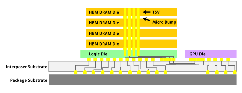
Applications of HBM
HBM, as a form of 3D stacked memory with significantly higher bandwidth than traditional planar memory, is used in the following applications:
Graphics Cards
- GPUs (Graphics Processing Units) handle large amounts of data during image and video rendering.
- HBM reduces performance bottlenecks with its high bandwidth.
High-Performance Computing (HPC)
- Supercomputers and specialized data centers rely on HBM for executing complex calculations and simulations quickly.
Deep Learning and AI
- Neural networks require massive data processing and fast computation.
- HBM maximizes the performance of AI chips with its high bandwidth.
Advantages for These Applications
- High Bandwidth and Low Latency:
- Wide interface width and shortened signal paths enable fast data access.
- Improved Energy Efficiency:
- Consumes less power for the same data transfer amount.
In recent years, HBM demand has surged, especially for AI GPUs packaged with silicon interposers, as used in generative AI applications.
HBM package layout from a top view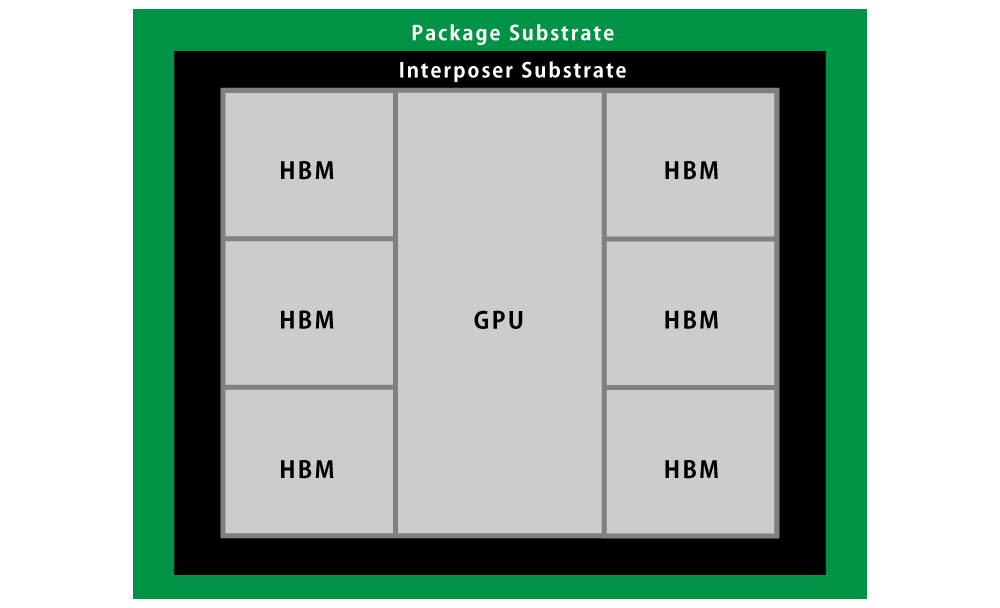
Challenges and Future Prospects of HBM
Challenges
- Cost:
- HBM manufacturing involves TSV technology and intricate stacking processes, making it costly.
- However, as manufacturing processes mature and scale increases, costs are expected to decline.
- Thermal Management:
- HBM’s multi-layer stacking structure can concentrate heat, creating cooling challenges.
- Innovative cooling technologies and optimized thermal designs are being explored to address this.
Future Prospects
HBM plays a vital role in advanced applications that require high bandwidth and energy efficiency. As the technology progresses:
- Cost Reductions:
- Lower costs will expand HBM adoption beyond high-performance applications like AI and gaming to include fields such as VR, autonomous vehicles, and other emerging applications.
- Enhanced Cooling Solutions:
- Advances in thermal management will further enable HBM use in energy-intensive environments.
HBM is poised to remain a cornerstone of high-performance computing and will continue to evolve to meet the growing demands of advanced technologies.
Glossary
- DDR (Double Data Rate): A type of DRAM where data is transferred on both the rising and falling edges of the clock signal, effectively doubling the data transfer rate.
- Interface Width: Refers to the number of bits that can be transferred in one data transaction. Wider interfaces allow more data to be transferred at once.
- Memory Cell: The smallest unit in a memory device that stores data, typically made up of transistors and capacitors.


 Contact Us
 Download documents
 Member services