- HOME
- News & Event
- News
- 【Spotlight】Revolutionizing AI Chips: an Embedded Component Substrate Explained
News & Event
News
2025/03/18
Column
【Spotlight】Revolutionizing AI Chips: an Embedded Component Substrate Explained
Among advanced semiconductor technologies, 3D integration significantly impacts future semiconductor performance alongside miniaturization. This article explains embedded component substrates, a key technology of 3D integration.
What is an Embedded Component Substrate?
An embedded component substrate is a technology that allows electronic components and circuit chips to be embedded inside a substrate rather than mounted on its surface. This innovation enables the miniaturization of devices and enhances performance.
Types of Components Embedded
Examples of components embedded in these substrates include:
- Resistors: Regulate current flow and set voltage levels.
- Capacitors: Store charge, filter power supply noise, and temporarily hold power.
- Inductors: Store energy using magnetic fields and provide resistance to current flow, commonly used in power management and filtering.
- Diodes: Restrict current flow to one direction and regulate voltage.
- Transistors: Used for switching and amplifying current.
Other integrated circuits (ICs) can also be embedded in the substrate. Each component is printed in specific areas of the substrate, then covered with insulation layers, eliminating the need for traditional surface-mounted components. This reduces device size and improves spatial efficiency.
Advantages
- Smaller Size: Embedding components reduces the overall size of devices.
- Improved Signal Transmission: Shortened signal paths reduce delays.
- Enhanced Reliability: Embedded components are better protected, improving the device’s durability and reliability.
Because of these benefits, embedded component substrates are widely used in compact, high-performance devices like smartphones, wearables, and high-frequency communication devices.
Example of an embedded component substrate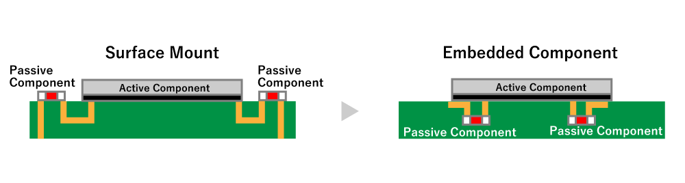
Applications of Embedded Component Substrates
One prominent application of embedded component substrates is AiP (Antenna-in-Package) technology.
What is AiP?
AiP integrates an RF chip and antenna into a single package. AiP comes in two types:
- Surface-Mount Type
- Embedded Type
The embedded type offers advantages over the surface-mount type, such as reduced signal loss, minimized noise interference, and improved device miniaturization. It is used in the following devices:
- Smartphones and Mobile Devices:
- Demands compactness and high performance.
- Embedded AiP enables efficient signal transmission and reliable wireless communication.
- Wearables (Smartwatches, Fitness Bands, Smart Glasses):
- Prioritizes miniaturization and comfort.
- Embedded AiP supports thin, flexible designs with high-quality signal transmission.
- IoT Devices:
- Includes sensor networks, smart home devices, and industrial sensors.
- Embedded AiP achieves device miniaturization and energy efficiency, enabling effective signal transmission.
Example of an AiP application in embedded substrates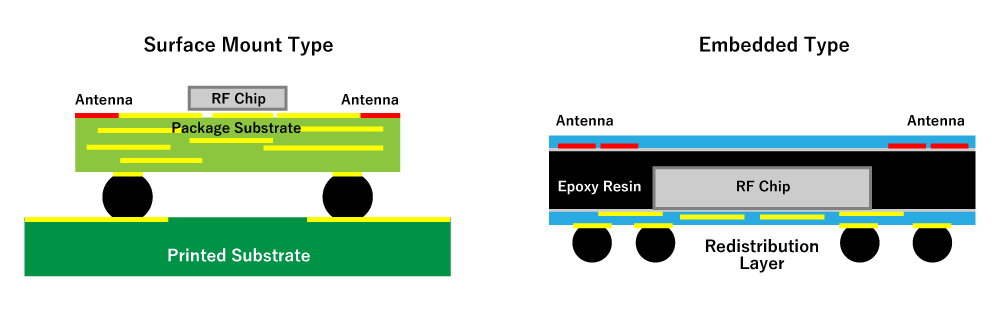
Future Prospects and Challenges
While embedded component substrates offer numerous advantages, they face the following challenges:
- Thermal Management
- Embedding components densely inside the substrate can lead to heat concentration and dissipation issues.
- Effective cooling designs and heat management strategies are essential.
- Manufacturing Technology
- Advanced manufacturing technologies and equipment are required for processes like embedding, wiring, and substrate drilling.
- There is a need to enhance manufacturing efficiency while reducing costs.
- Design Complexity
- Designing embedded component substrates involves optimizing component placement, signal paths, and minimizing interference.
- Issues like signal crosstalk and noise require advanced design methodologies and simulations.
Future Outlook
Despite these challenges, embedded component substrates are crucial for enabling high-density component integration and high-frequency signal transmission. They are expected to find broader applications in HPC (High-Performance Computing) and automotive communication devices, offering high-speed and reliable data transmission while minimizing signal delays and noise.
Glossary
- Integrated Circuit (IC): A device that integrates multiple electronic components, such as transistors, resistors, and capacitors, onto a silicon chip.
- High-Frequency Communication Devices: Devices that operate in high-frequency bands (e.g., tens of kHz to tens of GHz), used in applications like wireless communication, satellite systems, and mobile networks.
- Antenna-in-Package (AiP): A technology that integrates an antenna into a semiconductor package, improving signal transmission and device compactness.
- Signal Crosstalk: Interference caused by electrical signals from one circuit affecting neighboring circuits, often occurring in closely packed signal paths.


 Contact Us
 Download documents
 Member services