- HOME
- News & Event
- News
- 【Spotlight】Revolutionizing AI Chips: Hybrid Bonding Explained
News & Event
News
2025/03/18
Column
【Spotlight】Revolutionizing AI Chips: Hybrid Bonding Explained
Among advanced semiconductor technologies, 3D integration plays a crucial role in shaping the future performance of semiconductors alongside miniaturization. This article explains Hybrid Bonding, a core technology of 3D integration.
What is Hybrid Bonding?
Hybrid Bonding is a semiconductor packaging technology that connects metal pads on two or more semiconductor devices (typically ICs) directly without the use of Cu bumps. This eliminates spatial limitations imposed by bump size, enabling a significantly higher number of interconnects.
Hybrid Bonding is used when the interconnect pitch is less than 10 µm.
Why Hybrid Bonding Is Expanding
The demand for Hybrid Bonding is growing in advanced semiconductor devices, such as those used in HPC (High-Performance Computing), due to the need for increased computing power and interconnect density. Advanced processors are designed to handle complex, data-intensive tasks like simulations and data processing. To meet these demands, high-speed and efficient communication between components such as processors, memory, and accelerators is essential.
Compared to conventional wire bonding or flip-chip technologies, Hybrid Bonding offers:
- Higher interconnect density
- Shorter wiring distances, improving electrical performance and reducing power consumption and communication delays.
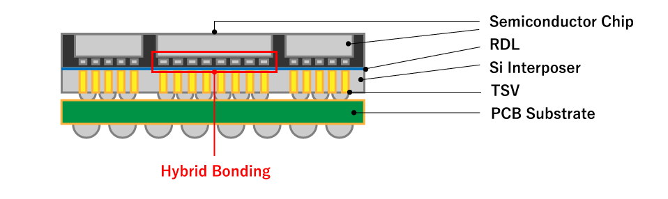
For these reasons, Hybrid Bonding is increasingly adopted in HPC and HBM (High Bandwidth Memory) applications.
Comparison of chip connection methods and bump sizes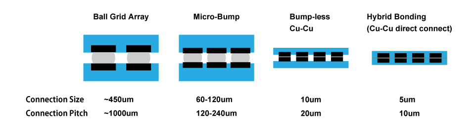
Hybrid Bonding Stacking Process
Currently, there are two primary methods for stacking semiconductor devices using Hybrid Bonding:
- W2W (Wafer-to-Wafer):
Both the top and bottom semiconductor devices remain in wafer form during stacking.- Advantages: Higher productivity due to batch processing.
- Disadvantages: Lower yield since defective chips cannot be selected.
- D2W (Die-to-Wafer):
The top semiconductor device is diced into individual dies and then stacked onto the bottom wafer.- Advantages: Higher yield due to the ability to select good chips.
- Disadvantages: Lower productivity because chips are processed one by one.
A hybrid approach combining the benefits of both methods—where good chips are picked and placed onto a wafer before wafer-to-wafer bonding—is also being explored.
Illustration of W2W and D2W methods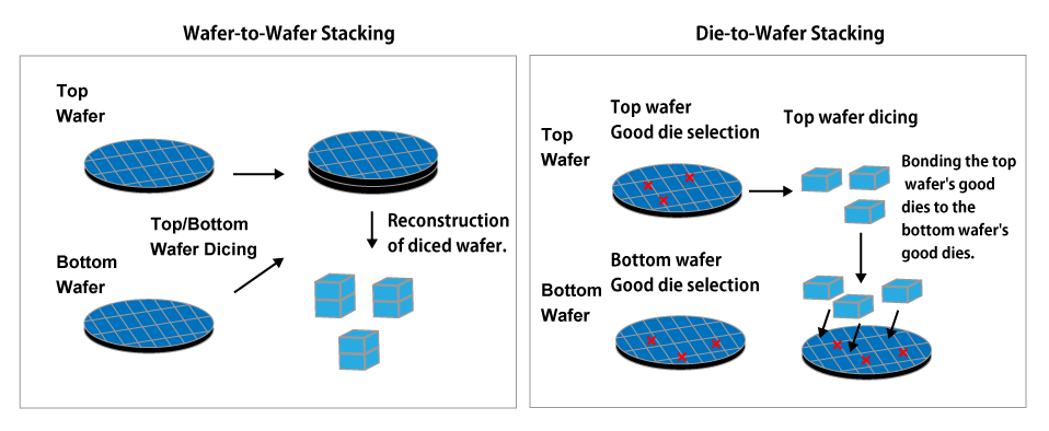
Wafer-to-Wafer Stacking
- Top Wafer and Bottom Wafer remain in wafer form.
- The top and bottom wafers are aligned and bonded together.
- After bonding, the combined wafer is diced into individual chips.
Die-to-Wafer Stacking
- Top Wafer:
- Good dies are identified and selected from the wafer.
- The selected dies are diced.
- Bottom Wafer:
- Good dies are identified and marked on the wafer.
- The selected good dies from the top wafer are individually bonded to the good dies on the bottom wafer.
Hybrid Bonding Joining Process
The Hybrid Bonding joining process involves bonding two semiconductor wafers or dies using a combination of metal and dielectric materials. Typically, copper (Cu) is used for electrical wiring, while dielectric materials like silicon dioxide (SiO₂) or silicon nitride (SiN) provide insulation.
Key Steps in the Process:
- Surface Preparation:
- The wafers or dies are cleaned to ensure proper adhesion and electrical contact between the metal and dielectric materials.
- Processes like CMP (Chemical Mechanical Polishing) and chemical cleaning are used.
- Alignment and Bonding:
- Precise alignment is performed using specialized equipment to ensure the metal interconnects make accurate contact.
- After alignment, temperature, pressure, and sometimes an electric field are applied to form strong chemical and mechanical bonds.
- Post-Bond Annealing:
- The bonded wafers or dies are heated to strengthen the bond and improve overall reliability.
- Singulation and Packaging:
- The bonded wafers or dies are diced into individual ICs, which are then packaged and tested before shipment.
Illustration of the Hybrid Bonding joining process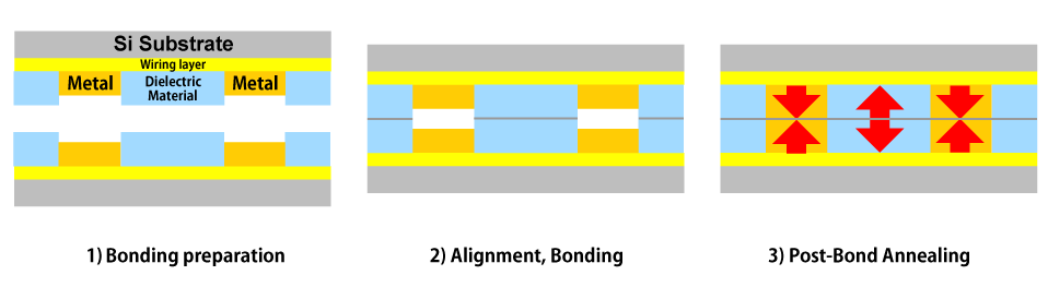
Challenges of Hybrid Bonding
Despite its advantages, Hybrid Bonding is a relatively new technology with several challenges:
- Precision Alignment:
Achieving precise alignment for interconnects with pitches smaller than 10 µm is difficult. - Surface Preparation:
The quality and cleanliness of surfaces are critical to ensuring strong and reliable bonds. - Process Control and Yield:
Advanced process control is necessary to maintain high yield during production. - Thermal-Mechanical Stress:
Differences in thermal expansion between materials can create stress, potentially leading to defects. - Testing and Repair:
The high-density interconnects and complex structures make testing and repairing Hybrid Bonding challenging. - Cost:
The need for specialized equipment and processes increases production costs.
Future Outlook
Hybrid Bonding is a critical technology for next-generation semiconductor devices due to its ability to enhance interconnect density, performance, and power efficiency while reducing form factors. Continued innovation in materials, processes, and equipment will help address current challenges, enabling broader adoption across industries.
Glossary
- Metal Pad: Small metal regions on chips that enable electrical connections.
- Cu Bump: Copper structures used in flip-chip packaging to directly connect chips to substrates.
- Interconnect: Electrical wiring or conductors that connect components within a semiconductor device.
- HBM (High Bandwidth Memory): A type of DRAM that uses 3D-stacked memory chips connected via TSVs for high-speed data transfer.
- Dielectric Material: Insulating materials used to control charge movement in semiconductor devices.
- Form Factor: The physical size, shape, and space requirements of a semiconductor device.


 Contact Us
 Download documents
 Member services