- HOME
- News & Event
- News
- 【Spotlight】Revolutionizing AI Chips: PLP Technology Explained
News & Event
News
2025/03/18
Column
【Spotlight】Revolutionizing AI Chips: PLP Technology Explained
Among advanced semiconductor technologies, 3D integration significantly impacts future semiconductor performance alongside miniaturization. This article explains PLP (Panel Level Package) technology, a key component of 3D integration.
What is PLP Technology?
PLP (Panel Level Package) is an extension of the FOWLP (Fan-Out Wafer Level Package) mass production concept, applying it to larger panel-sized substrates instead of wafers.
In FOWLP, multiple silicon dies are mounted onto a 300 mm wafer, enabling batch manufacturing of packages, which significantly reduces per-package production costs. PLP applies this batch manufacturing approach to larger panel substrates, such as printed circuit boards or glass substrates.
Panel Substrate Size Comparison
For example, printed circuit boards measuring 610 mm × 457 mm have approximately 4 times the area of a 300 mm wafer (707 mm² vs. 2788 mm²). This means that, theoretically, 4 times as many packages can be manufactured in a single batch. Additionally, since chips are square, arranging them on a rectangular panel substrate minimizes wasted space compared to circular wafers.
PLP uses an RDL (Redistribution Layer) to connect chip terminals, similar to FOWLP. However, while the L/S (line/space) of FOWLP’s RDL is below 5 µm, PLP’s L/S is 10 µm or above, limiting its ability to form fine wiring. This limitation arises because the larger substrate size makes it more susceptible to thermal expansion, making it difficult to achieve uniform RDL formation over a large area. Consequently, PLP is primarily used for packaging legacy semiconductors with fewer pins.
Size comparison between wafer substrate and panel substrate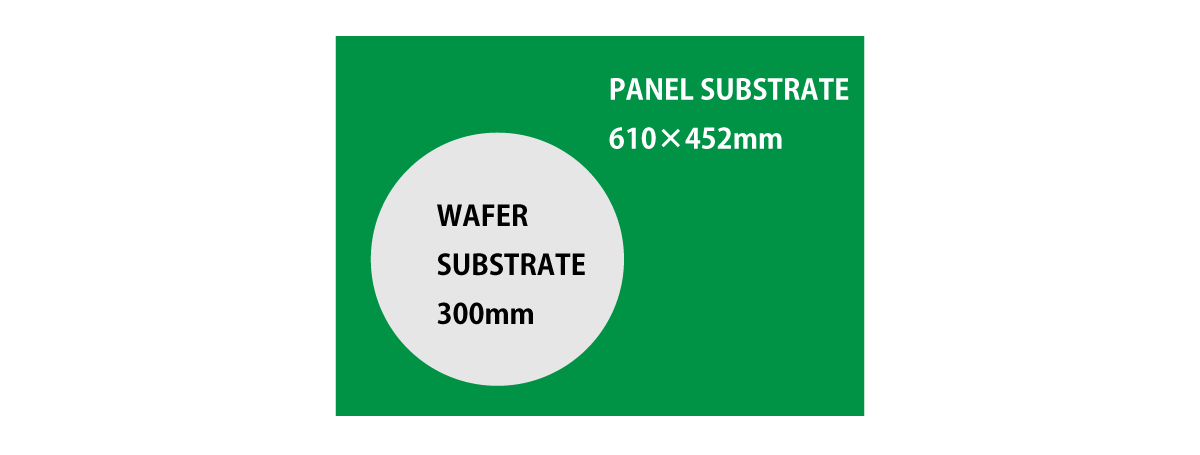
PLP Fabrication Processes
PLP manufacturing begins with selecting good dies from a wafer using a pick-and-place process, placing them in designated positions on a panel substrate. RDL formation can occur in one of two ways, depending on the timing of the process:
- MOLD First Process:
- After placing chips on the substrate, they are encapsulated with MOLD resin, followed by RDL layer formation.
- RDL First Process:
- The RDL layer is formed on the panel substrate before chips are placed, with chips subsequently encapsulated using MOLD resin.
Chip Orientation in MOLD First Process
In the MOLD First process, chips can be oriented in two ways:
- Face-Down: The chip circuit side faces the panel substrate.
- Face-Up: The chip circuit side faces upward, away from the panel substrate.
Both MOLD First and RDL First processes have their advantages and disadvantages. The choice of process depends on factors like chip characteristics and manufacturing requirements.
PLP pick-and-place process illustration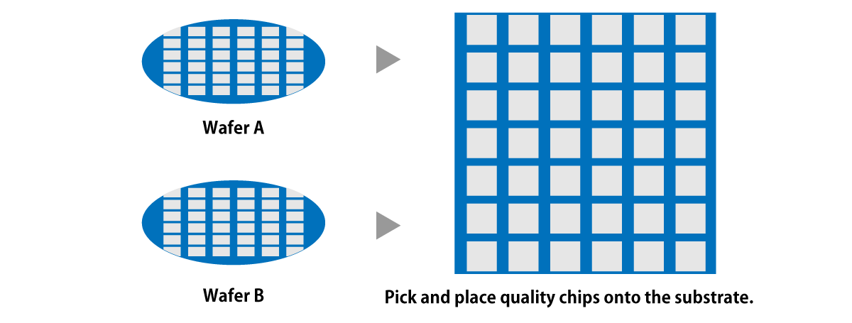
Challenges of PLP Technology
PLP offers the advantage of reduced costs by enabling batch manufacturing of a larger number of chips compared to FOWLP. However, it faces several challenges:
- Lack of Standardization:
The large panel size introduces variability, and industry-wide standards for panel dimensions and processes have yet to be established. - Equipment and Process Development:
Machinery and processes for handling and processing large panels are still under development. - Die Shift Issues:
Die shift refers to chips placed on the panel substrate deviating from their intended positions. Causes include thermal expansion and minor errors during processing.
Despite these challenges, as RDL refinement progresses, PLP technology is expected to support advanced devices and expand its applications. For instance, legacy semiconductors used in EVs requiring high-density integration may benefit from PLP in the future.
Glossary
- Printed Circuit Board (PCB): A substrate used for electrical circuits. It features pre-designed circuit patterns printed on a conductive metal foil attached to the substrate.
- MOLD Resin: A type of resin used in semiconductor manufacturing. “MOLD” stands for “Molded Plastic Package,” referring to resin-encased packages.


 Contact Us
 Download documents
 Member services