- HOME
- News & Event
- News
- 【Spotlight】Revolutionizing AI Chips: TSV Technology Explained
News & Event
News
2025/03/18
Column
【Spotlight】Revolutionizing AI Chips: TSV Technology Explained
Among advanced semiconductor technologies, 3D integration plays a crucial role in shaping the future performance of semiconductors alongside miniaturization. This article explains TSV (Through-Silicon Via) technology, a key component of 3D integration.
What is TSV Technology?
TSV (Through-Silicon Via) refers to a technique that creates through-silicon electrodes. Instead of traditional Cu wire bonding to electrically connect chips, TSV involves drilling narrow holes (vias) through silicon wafers, filling them with metal to create electrodes, and electrically and mechanically connecting silicon chips through micro-bumps.
Key Benefits of TSV Technology:
- Faster Processing Speeds:
TSV shortens the distance between chips compared to wire bonding, enabling high-speed signal transmission and supporting higher pin counts. - Miniaturization and High Density:
TSV allows for stacking multiple chips into a single package, reducing overall package size. Unlike wire bonding, it eliminates protruding wires, further minimizing area usage. - Low Power Consumption:
TSV reduces signal transmission distances, decreasing wiring resistance and lowering power consumption.
Current Applications:
TSV technology is widely used in stacked image sensors, HBM (High-Bandwidth Memory), and silicon interposers. It is also expected to enable the vertical connection of heterogeneous chips for future 3D ICs.
Comparison between wire bonding and TSV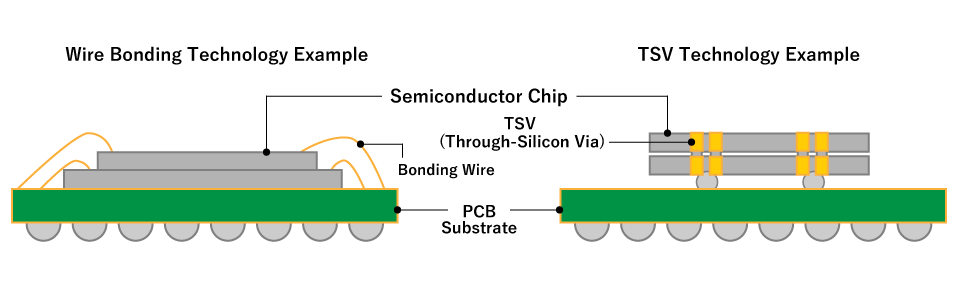
Types of TSV Fabrication Processes
There are several types of TSV via fabrication processes, but the most common are via-middle and via-last processes.
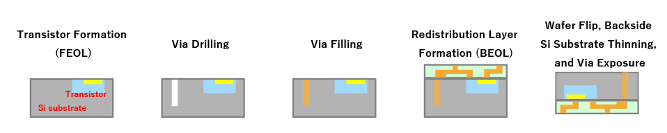
- Via-Middle Process:
This process occurs during the BEOL (Back-End-Of-Line) wiring stage, where vias are created using wafer fabrication techniques. Typically performed by foundries, which handle the early-stage wafer processes. - Via-Last Process:
In this process, after completing all FEOL (Front-End-Of-Line) and BEOL wiring, the wafer is thinned, supported, and vias are created. This is typically performed by OSAT (Outsourced Semiconductor Assembly and Test) companies specializing in assembly and testing.
Step-by-step fabrication process for via-middle and via-last methods
Via-Middle Process
Via-Last Process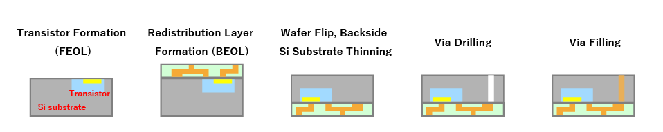
Challenges of TSV Technology
Compared to traditional wire bonding, TSV and micro-bump technologies are relatively new and more complex, resulting in higher manufacturing costs.
- High Production Costs:
-
- TSV requires etching to drill holes and the formation of an insulating layer to isolate Si and Cu. This increases both process and material costs.
- Thermal Expansion Issues:
-
- TSV involves thinning the Si substrate to reduce stress (e.g., to 50 µm). However, differences in thermal expansion rates between Cu electrodes and Si substrate layers can concentrate stress, causing defects or fractures within the chip.
- Reliability Concerns:
-
- TSV’s relatively short history in mass production limits its long-term reliability.
- Electrical characteristics, such as increased inductance and capacitance, can lead to signal delays and attenuation.
- Material degradation, such as insulation layer wear, could further impact chip reliability over time.
Despite these challenges, TSV technology is critical for achieving faster, more compact, and energy-efficient semiconductors. Semiconductor device manufacturers, material suppliers, and equipment makers are collaborating to address these issues and improve the technology.
Glossary
- BEOL (Back-End-Of-Line): Refers to the later stages of semiconductor manufacturing, including the formation of wiring and protective layers after circuit creation on the wafer.
- Foundry: A company specializing in semiconductor manufacturing for fabless companies based on their designs.
- FEOL (Front-End-Of-Line): Refers to the early stages of semiconductor manufacturing, including the formation of transistors.
- OSAT (Outsourced Semiconductor Assembly and Test): Companies that specialize in semiconductor assembly and testing, often working with foundries that handle wafer production.


 Contact Us
 Download documents
 Member services