- HOME
- News & Event
- News
- 【Spotlight】Revolutionizing AI Chips: Advanced Package Integration Explained
News & Event
News
2025/03/18
Column
【Spotlight】Revolutionizing AI Chips: Advanced Package Integration Explained
What is a Semiconductor Package Substrate?
A semiconductor package substrate is used to transmit electrical signals between semiconductor chips and printed circuit boards (PCBs).
The main types of semiconductor package substrates are:
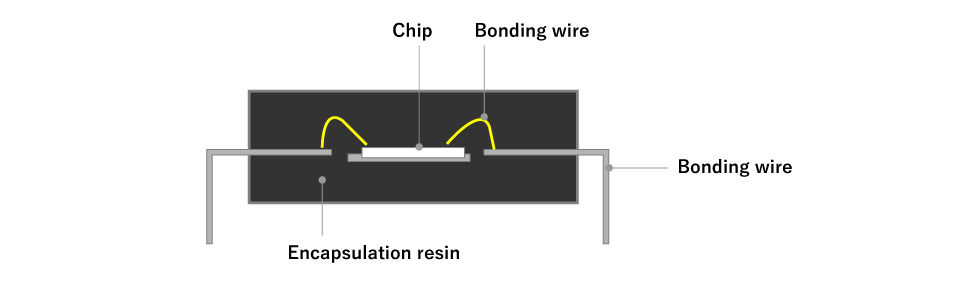
- Lead Frame Type
- Connects the semiconductor chip to the lead frame using wire bonding*², which is then connected to the mainboard.
- Commonly used in power devices.
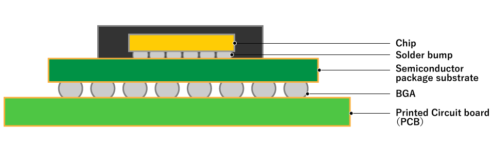
- Laminated Substrate Type
- Forms solder bumps on the chip side, connecting them to the circuits on the semiconductor substrate (flip-chip mounting).
- The semiconductor substrate and PCB are connected via BGA (Ball Grid Array)*³.
- Allows for miniaturization and higher pin counts, making it suitable for SoC (System on Chip) applications.
Laminated substrates are more densely packed for chip mounting and use the semi-additive process (SAP)*¹ for circuit miniaturization.
Side view diagram of wire bond mounting (side view)
Side view of flip-chip (FC) implementation
Current Mainstream Advanced Packaging Technologies
In recent years, advanced semiconductor chips used in smartphones and HPC systems have increasingly required higher speeds, lower power consumption, and compactness. As a result, advanced semiconductor package substrates must meet these three key points:
- Miniaturization through high-density mounting
- Higher pin counts due to multifunctionality
- High performance with enhanced thermal dissipation and electrical characteristics
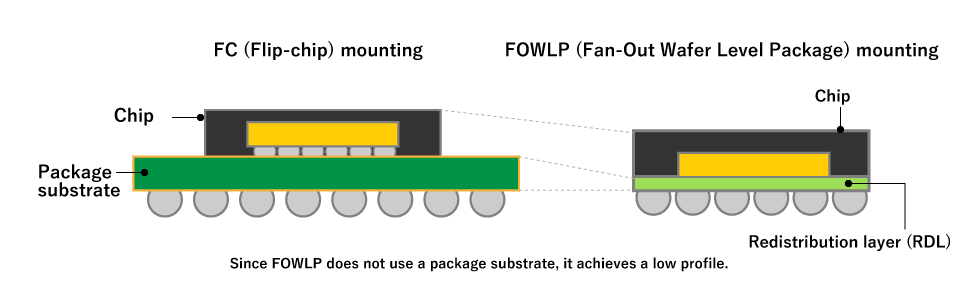
To meet these demands, new packaging technologies have been introduced, the most representative being FOWLP (Fan-Out Wafer Level Package).
This technology is based on WLCSP (Wafer Level Chip Scale Package)*⁴ and uses front-end manufacturing techniques to expand the redistribution layer beyond the chip area, increasing the number of connection terminals to support higher pin counts.
Solder bumps are directly formed on the redistribution layer, eliminating the need for semiconductor package substrates required in flip-chip mounting. This results in an even thinner overall package compared to flip-chip mounting.
Comparison of package heights: Flip-chip (FC) vs. FOWLP
Comparison of terminal positions: Conventional WLP vs. Fan-out WLP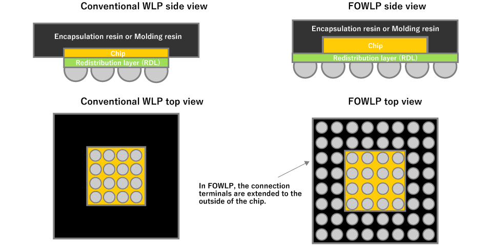
Challenges of FOWLP
The challenges of FOWLP are as follows: while it is currently used primarily for mobile applications due to its thin profile, future demand is expected to grow in areas requiring high integration, such as HPC and AI. Specific challenges include:
- Adapting to multi-chip and chiplet configurations
- Enhancing thermal dissipation and durability for automotive applications
In recent years, new technologies have emerged, such as mounting FOWLP chips on interposer substrates to achieve high integration. For automotive applications, where environmental conditions are harsh, it is necessary to improve heat dissipation and durability.
By combining FOWLP with existing packaging and interposer technologies, it is expected to be used in a wide range of applications and drive the evolution of semiconductor packaging technology.
Glossary
- SAP (Semi-Additive Process): A method that uses photolithography to form wiring patterns on the surface of a PCB. UV light is used to create bonding pads and wiring patterns for connecting semiconductor chips.
- Wire Bonding: A method of electrically connecting semiconductor chips to lead frames using wires made of gold, aluminum, or copper.
- BGA (Ball Grid Array): A type of surface-mount packaging for integrated circuits, connecting chips and PCBs via solder balls on the package’s backside.
- WLCSP (Wafer Level Chip Scale Package): A method where semiconductor packaging is completed on the wafer itself, allowing for minimal package size to match the chip size.


 Contact Us
 Download documents
 Member services