- HOME
- News & Event
- News
- 【Spotlight】Revolutionizing AI Chips 2.5D Integration Technology Explained
News & Event
News
2025/03/18
Column
【Spotlight】Revolutionizing AI Chips 2.5D Integration Technology Explained
Among advanced semiconductor technologies, 3D integration significantly impacts future semiconductor performance alongside miniaturization. This article explains 2.5D integration technology, a foundational aspect of 3D integration.
Background of 2.5D Integration Technology Expansion
Since the invention of transistors, semiconductor growth has been driven by Moore’s Law, which states that the number of transistors on a single chip doubles approximately every two years.
This principle led to significant reductions in system manufacturing costs and performance improvements, such as higher operating frequencies. Technologically, advancements in monolithic IC manufacturing allowed for the integration of multiple functions onto a single chip, known as System on a Chip (SoC).
However, as Moore’s Law slowed, the cost per chip increased, reducing the benefits of packing more transistors into one chip.
To extend Moore’s Law, a new generation of packaging technology emerged: integrating multiple chiplets (non-monolithic semiconductor chips) into a single package. This system integration technology has been adopted in advanced applications, such as smartphones and High-Performance Computing (HPC) systems.
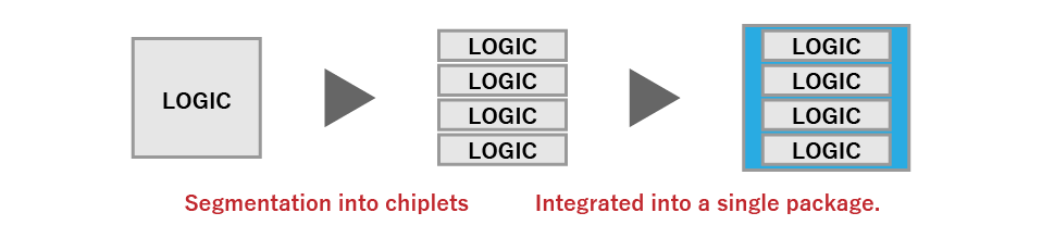
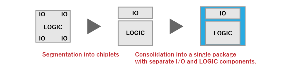
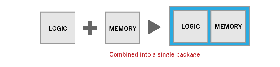
Three Examples of Packaging with Multiple Semiconductor Chips
- Chip Function Segmentation and Package Integration
- Chip Function Consolidation and Package Integration
- Heterogeneous Chip Package Integration
Key Technologies Required for 2.5D Integration
The latest packaging technologies aim to:
- Minimize overall size to resemble a single chip.
- Reduce power consumption.
- Enhance performance.
- Accommodate multiple functions in one package.
2.5D integration achieves this through an interposer substrate. This technique places multiple silicon dies side-by-side in close proximity on a substrate. For high-performance semiconductors, silicon interposers are primarily used.
Key features of a silicon interposer include:
- Redistribution Layer (RDL): Multi-layer wiring circuits on the surface that electrically connect the chips.
- Through-Silicon Vias (TSVs): Vertical electrical connections between the interposer and the underlying substrate.
The advantage of using a silicon interposer lies in its ability to replicate SoC-level performance by minimizing the distance between chips. Additionally, silicon interposers enable the formation of fine wiring (RDL), which is challenging with resin-based substrates. The silicon base also reduces warping caused by differences in thermal expansion, making it possible to integrate multiple chips efficiently.
A conceptual side view diagram of 2.5D integrated semiconductor chips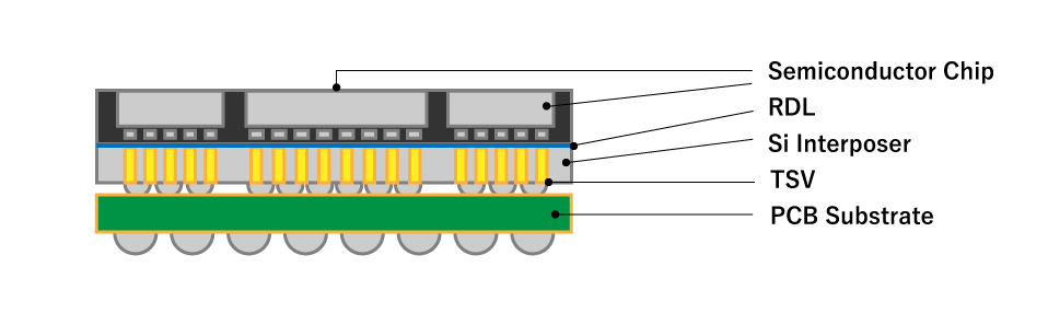
Challenges of 2.5D Integration Technology
The primary challenges of 2.5D integration with silicon interposers are cost and implementation area.
- Advanced silicon interposers can reach areas as large as 3,400 mm² (approximately 58.6 mm per side), significantly increasing material costs.
- Additional costs arise from complex wiring processes and fine-pitch bumps required to connect silicon dies and interposers.
To reduce costs:
- Alternatives like resin-based interposers are being developed.
- Combined 2.5D and 3D integration techniques are gaining traction to reduce implementation areas.
As demand for edge computing grows, there is a need to develop cost-effective manufacturing processes tailored to specific applications.
Glossary
- SoC (System on a Chip): An integrated chip consolidating essential electronic circuits, including CPU, memory, and I/O interfaces, into a single unit.
- Monolithic IC: An electronic circuit that combines multiple functions into a single chip, exemplified by SoCs.
- Chiplet: A system of individual semiconductor chips designed to function together in a single package.
- Redistribution Layer (RDL): A layer of wiring that electrically connects chips to external substrates.
- Through-Silicon Via (TSV): Vertical electrical connections that pass through silicon wafers to enhance wiring density and reduce connection lengths.


 Contact Us
 Download documents
 Member services