
Wafer Visual Inspection System
by Tokyo Electron Device
Bring innovation
to your semiconductor production line

Are You Facing These Challenges?
Common Challenges
in the Field
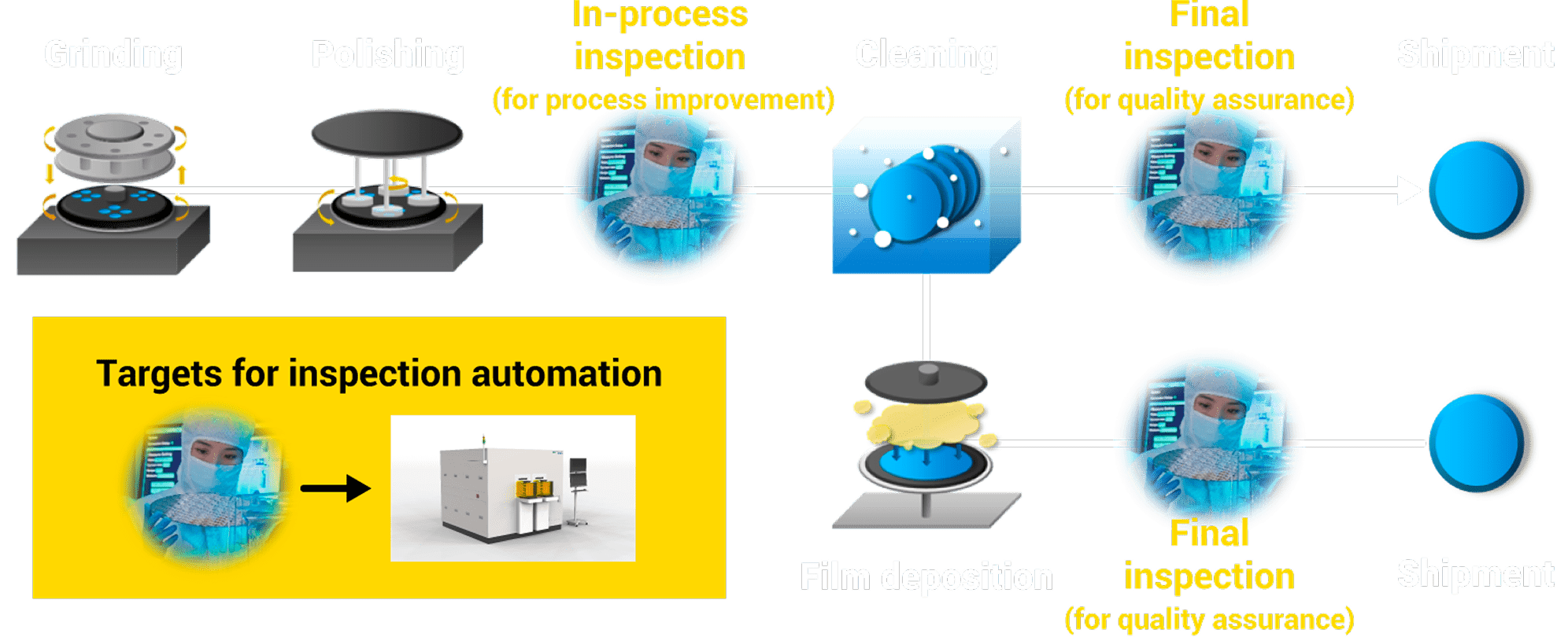
- Want to automate visual inspection
in high-volume production lines - Need to automate microscope-based
sample inspection - Want to replace aging inspection
equipment
Are
You
Facing
These
Challenges?
Common Challenges
in Inspection
- Want to perform 100% inspection
with high throughput - Need to inspect front side, back side
and edge of
the wafer in a single
process for better efficiency - Want to automatically classify defect types and
use the data
to drive process improvement
Quality and
Efficiency
Tokyo Electron Device
offers the solution.
Our cutting-edge inspection
technology
effectively
addresses all of these issues.
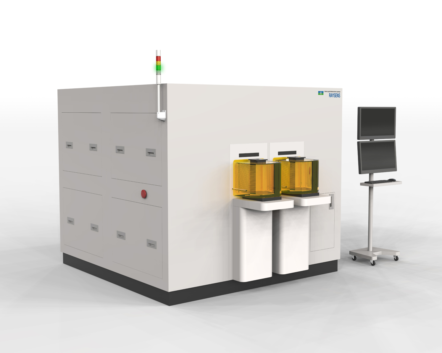
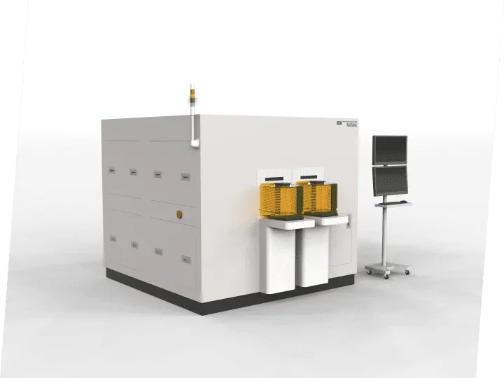
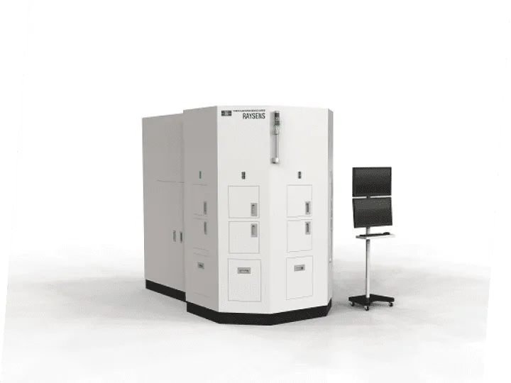
Wafer Visual
Inspection System
-
High-speed detection of submicron-level defects*40~120/wph
-
Multi-surface inspection (front, back, and
edge) with a single system -
Advanced image processing and AI for
defect detection and automatic
classification
Three Key Technologies
for Solving Inspection Issues
Technology
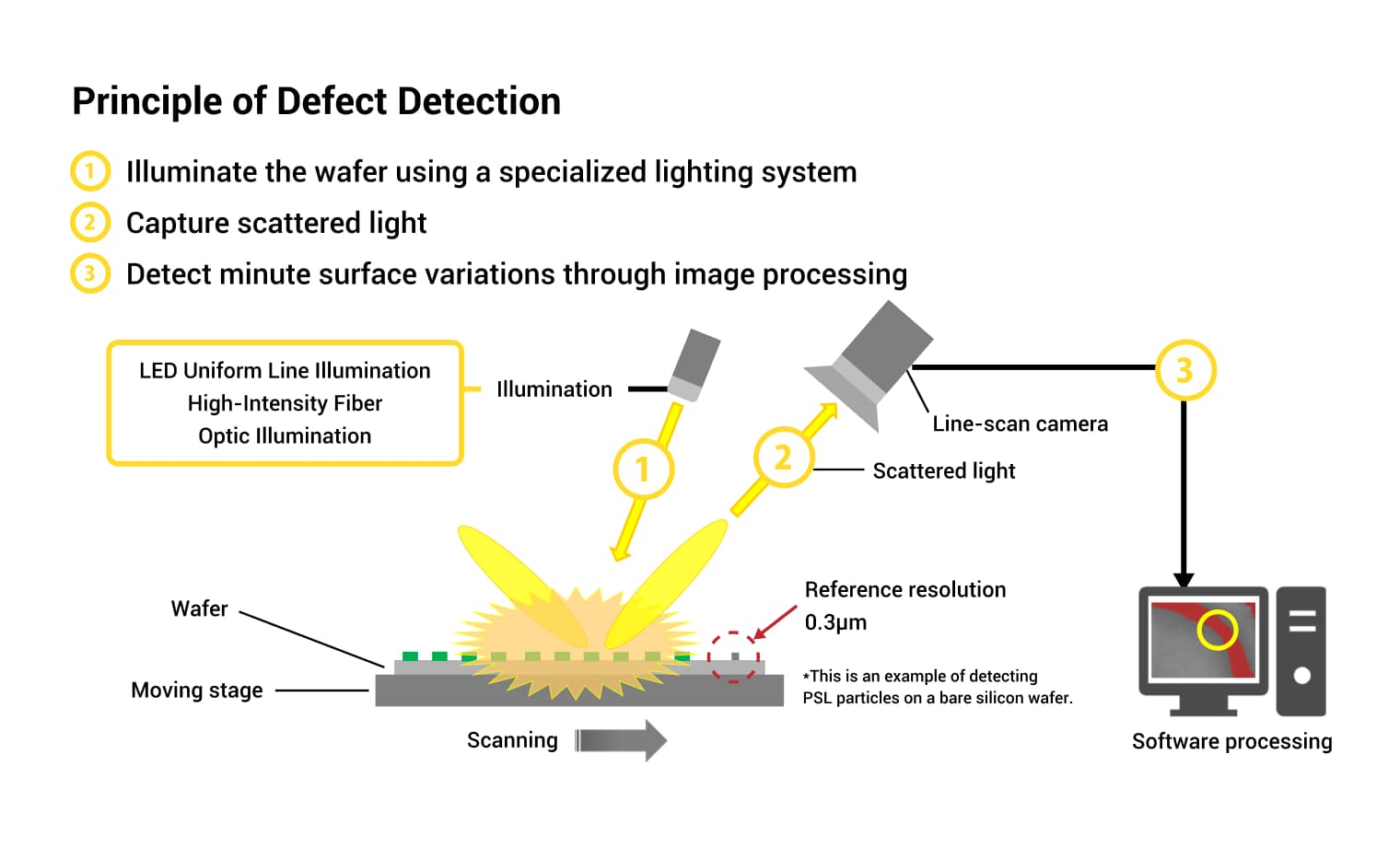
High-Speed, High-Sensitivity
Macro Inspection
Our specially developed optical system detects even subtle changes in light to identify defects.
It enables high-speed, high-sensitivity detection of particles, scratches, film irregularities,
and slip defects on wafers made of silicon, compound semiconductors, glass, and more.
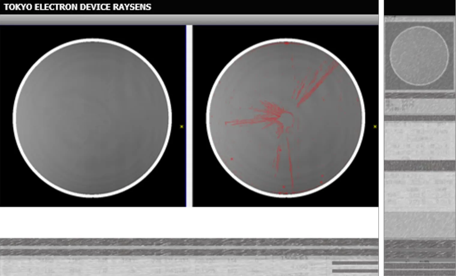
High-Performance Inspection Application
This integrated application manages inspection settings, recipe creation, and equipment control.
It detects target defects using optimized algorithms and automatic defect classification makes it easier to investigate and analyze the cause of defect.
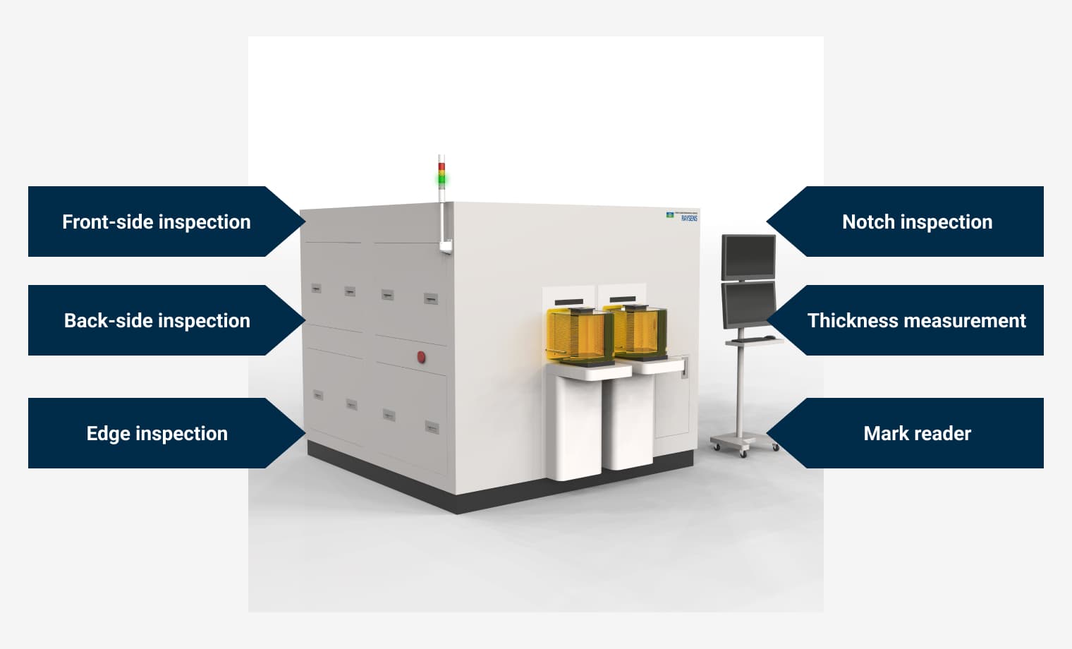
Multi-Function Architecture
(Front, Back, and Edge Inspection)
By integrating front surface, back surface, and edge inspection into a single system, this solution reduces the risk of particle contamination, shorten the total inspection time and save space.
Optional features such as wafer ID reading (OCR) and thickness measurement are also supported.
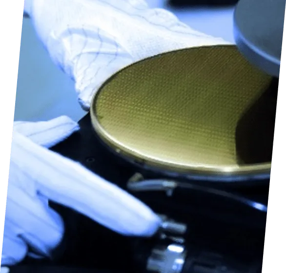
Applicable Wafers for
Inspection
Wafer
Our system supports a wide range of materials, including silicon wafers, compound wafers, glass wafers, and mask blanks.
We perform defect inspection using optical
systems and image processing tailored to the specific characteristics and defects of each
material.
-
Si(8/12inch)
Main Applications of Wafers
Widely used in various semiconductors such as logic and memory devices, as well as interposers.
-
SiC(6/8inch)
Main Applications of Wafers
For power semiconductor devices
(e.g., MOSFETs, Schottky Barrier Diodes (SBD), etc.) -
Glass(8/12inch)
Main Applications of Wafers
Support and carrier
wafers,
and interposer substrates -
LT/LN(6/8inch)
Main Applications of Wafers
SAW devices, optical isolators,
and sensors -
GaN(6/8inch)
Main Applications of Wafers
Power semiconductors for high voltage and high current, lasers, and LEDs
-
InP(3/4inch)
Main Applications of Wafers
Optical communication devices such as laser diodes, and high-
frequency devices -
Mask Blanks(6inch)


Defects Subject to
Inspection
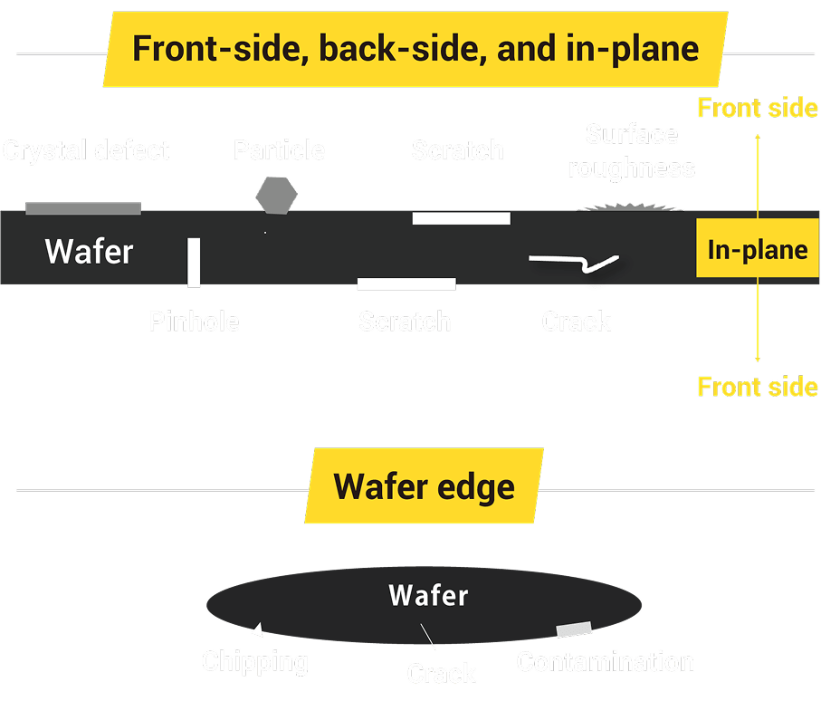
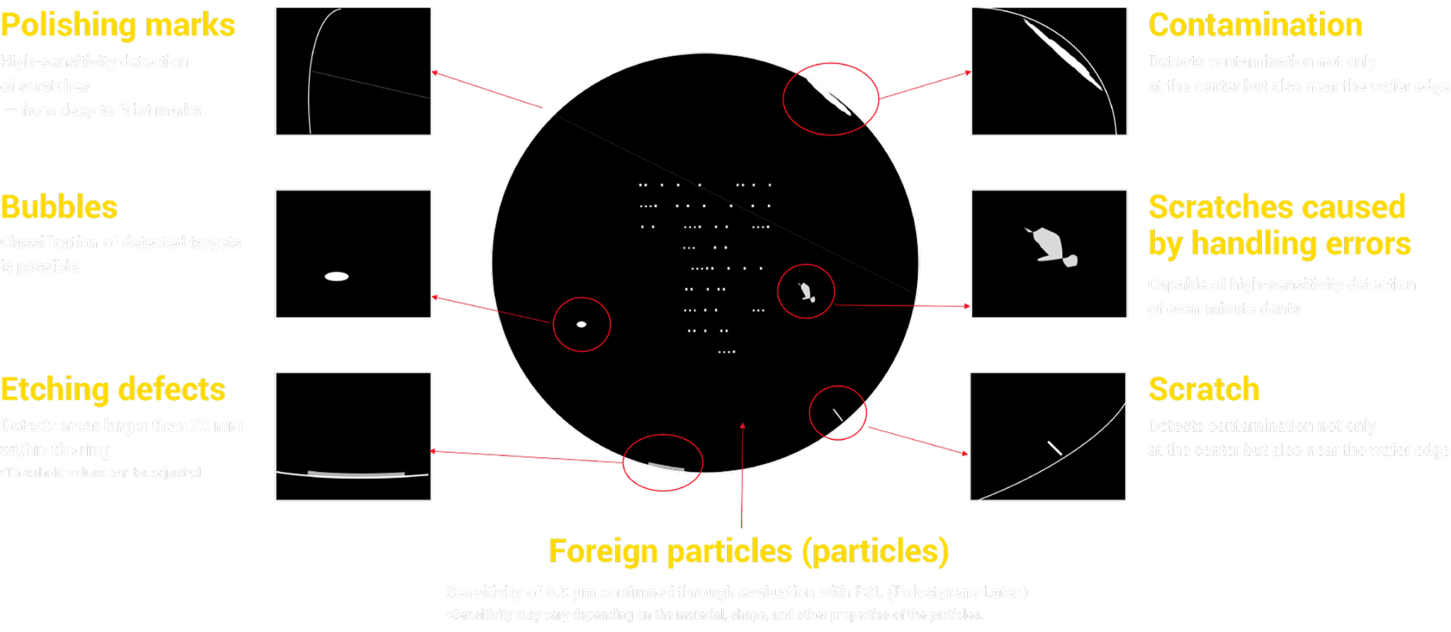
Defect
We inspect various types of defects shown in the diagram on the wafer’s front surface, in-plane,
back surface, and edge.
The primary target defect sizes range from submicron to several tens of microns.
List of Target Defects
| Category | Types of Defects to be Detected |
|---|---|
| Front surface / Back surface |
Foreign particles (Particles) |
| Contamination (Dirt) | |
| Scratches | |
| Dents (Dimples) | |
| Chips (Chipping) | |
| Cracks | |
| Crystal defects | |
| Pinholes | |
| Protrusions (Protuberances) | |
| Color non-uniformity | |
| Lithography defects (Litho defects) |
|
| Polish marks | |
| Grinding marks | |
| Thermal marks | |
| Haze | |
| Edge notch | Cracks / Chips / Contamination |
| Bonding surface | Voids |
Examples of Silicon and
Compound Semiconductor Wafers
Examples of Glass Wafers
Example of a Wafer Inspection Process
Inspection Process
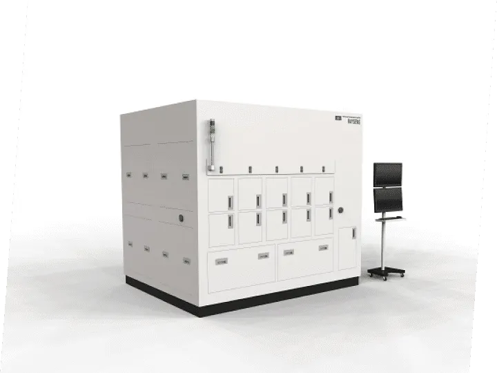
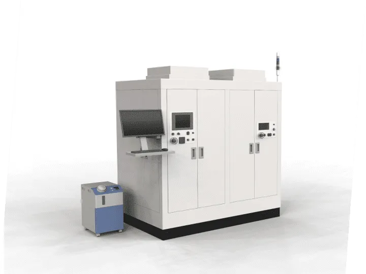
Inspection System Lineup
Line Up
We offer dedicated inspection systems tailored to specific inspection targets.
Each system is optimized—including inspection modules, optics, and image processing—to meet
your application needs and deliver a high-quality inspection environment.
-
Si wafer(6/12inch)
-
SiC wafer(6/8inch)
-
Glass wafer(8/12inch)
-
LT/LN wafer(6/8inch)
-
SiC latent crystal defect
-
Wafer Pattern Defect
Inspection Systems
Sample Evaluation Available

If you are facing inspection challenges, we offer sample evaluation using our in-house
test environment.
You can assess the feasibility of
inspection before moving forward with equipment implementation.
a Sample Evaluation
Download Materials for Free
-
01
Visual Inspection of Semiconductor Wafers

What You'll Learn from This
Guide:- ・Various types of wafer materials
- ・Wafer manufacturing processes and visual inspection
- ・Types of defects
- ・Categories of
inspection
technologies
Recommended For
Anyone interested in or facing challenges with the inspection of silicon (Si), compound semiconductors (SiC, GaN, LT/LN, InP), or glass wafers.
Recommended For
Anyone interested in or facing challenges with the inspection of silicon (Si), compound semiconductors (SiC, GaN, LT/
LN, InP), or glass wafers. -
02
The Next Dimension of Semiconductors:
Exploring Advanced Packaging
What You'll Learn from This Guide:
- ・Future trends in the market and technology
- ・Evolution of advanced packaging
- ・Solutions to wafer processing challenges
Recommended For
- ・Those who want to stay up-to-date on semiconductor market trends and advanced packaging technologies
- ・Professionals seeking solutions to challenges in manufacturing processes and wafer processing
- ・Individuals interested in high-speed, high-density manufacturing technologies
- ・Engineers and technical experts involved in next-generation semiconductor development
Feel Free to Contact Us
Start with a Trial!